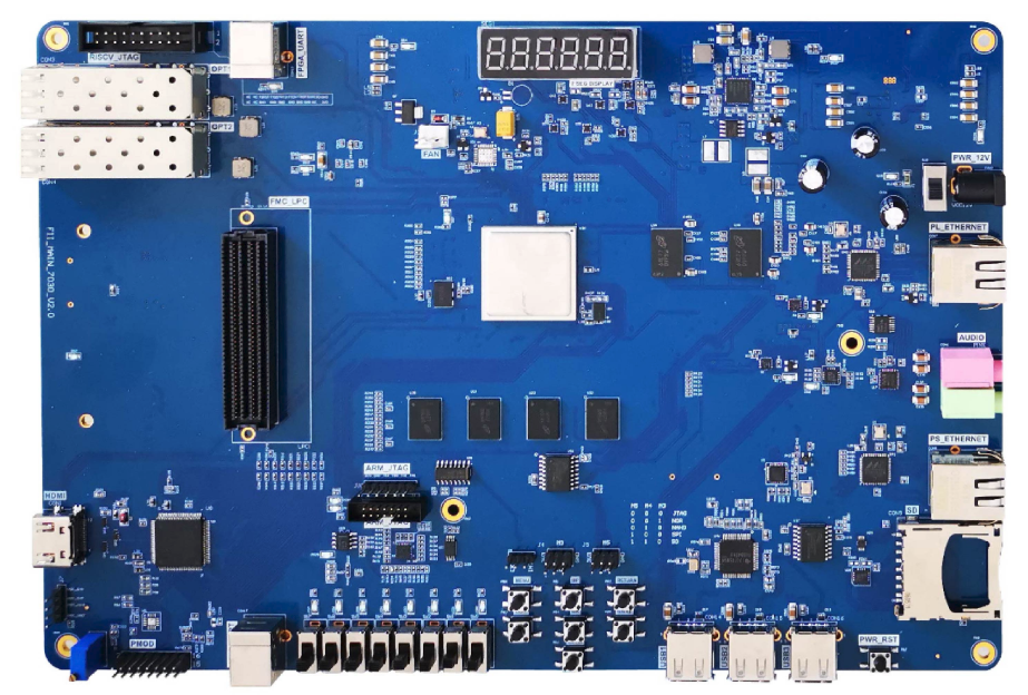
FII-PE7030 is a ready-to-use for educational platform which has been designed to cover FPGA development and experiment, ARM SOC development and experiment, network(copper or fiber) development ,digital communication and SDR(software define radio) with daughter board FII-BD9361 plug on.
Basic Experiment Functions:
FII-PE7030 xc7z030 zynq evb board is a ready-to-use for educational platform which has been designed to cover FPGA development and experiment, ARM SOC development and experiment, network(copper or fiber) development ,digital communication and SDR(software define radio) with daughter board FII-BD9361 plug on. It was designed for university students, teachers, and all other industrail professionals. FII-PE7030 is an incredibly flexible processing platform, capable of adapting to most of your project requires.
More surprising show up that recently Engineers has successful port RISC-V(RV32G) and RV64I to this platform, it becomes a real RISC-V SOC platform.
Application:
wireless Communication
DBC(digital base band communication) and DSP
SDR Software defined radio
LTE protocol analysis
4/5G base station
Network communication:
100M/1G ethernet communication both for PS and PL
10G SFP+ fibre communication with multiple protocol supported like LAN, SONET/SDH, CPRI etc.
Network switch and router
VLAN
Spanning Tree
USB:
1 480M high speed USB2.0 HUB
4 480M high speed USB2.0 connectors
CPU:
RISC-V CPU 32bit ecosystem development ,verification and validation
RISC-V CPU 64bit ecosystem development,verification and validation
Artificial Intelligence:
Audio or Voice Collection, Speech Recognition
Image Acquisition and Image Recognition, Deep Learning
FII-PRX100 Risc-V FPGA Board is a ready-to-use development platform designed around the Field Programmable Gate Array (FPGA) from Xilinx.
Open Source[edit]
There are many open-sourced RISC-V CPU designs, including:
The Berkeley CPUs. These are implemented in a unique hardware design language, Chisel, and some are named for famous train engines:
64-bit Rocket. Rocket may suit compact, low-power intermediate computers such as personal devices. Named for Stephenson’s Rocket.
The 64-bit Berkeley Out of Order Machine (BOOM). BOOM uses much of the infrastructure created for Rocket, and may be usable for personal, supercomputer, and warehouse-scale computers.
Five 32-bit Sodor CPU designs from Berkeley, designed for student projects. Sodor is the fictional island of trains in childrens’ stories about Thomas the Tank Engine.
picorv32 by Claire Wolf, a 32-bit microcontroller unit (MCU) class RV32IMC implementation in Verilog.
scr1 from Syntacore,a 32-bit microcontroller unit (MCU) class RV32IMC implementation in Verilog.
PULPino (Riscy and Zero-Riscy) from ETH Zürich / University of Bologna. The cores in PULPino implement a simple RV32IMC ISA for micro-controllers (Zero-Riscy) or a more powerful RV32IMFC ISA with custom DSP extensions for embedded signal processing.
It was designed to cover all aspects of FPGA Development and Experiment, RISC-V SOC .
The main application areas aim at smart home, Wearable, sensor Fusion, IOT, and industrial control etc.
FII-PRX100 Risc-V FPGA Board is a ready-to-use development platform designed around the Field Programmable Gate Array (FPGA) from Xilinx. It was designed to cover all aspects of FPGA Development and Experiment, RISC-V SOC . The main application areas aim at smart home, Wearable, sensor Fusion, IOT, and industrial control etc.
Features:
Fully supports the RV32IMFAC instruction architecture and provides a rich set of storage and interfaces, including: ITCM 64K(Instruction Tightly Coupled Memories) and DTCM 64K(Data Tightly Coupled Memories) for separate storage of instructions and data, and 2M bytes External super RAM support as well .
3-stage pipeline architecture
support machine mode only
From instruction fetch ,Decoder ,Execution to memory operation modules are 100% Manually developed by using pure verilog HDL, scalable and easy to be understood.
The flexible RISC-V IPCORE is suitable for customized ASIC for specific domain, Also can be used as embedded CPU within FPGA.
Interrupt controller, supports 16 high-priority, low-latency local vectored interrupts.
includes a RISC-V standard PLIC (platform-level interrupt controller ), which supports 127 global interrupts with 7 priority levels. provides the standard RISCV machine-mode timer and software interrupts via the CLINT(Core Local Interruptor)
2 UART
3 QSPI
I2C
3 PWM
10M/100M/1G ethernet
Watchdog
32 GPIO
4 7-seg display interface
External Serial Flash
Debug Interfaces: JTAG
12-Bit ADC
Four data lines I2S and can support maximum of 8 audio outputs or 4 stereo channels
Hardware Crypto Engine for Advanced Fast Security, Including: AES 128, CRC, Checksum etc
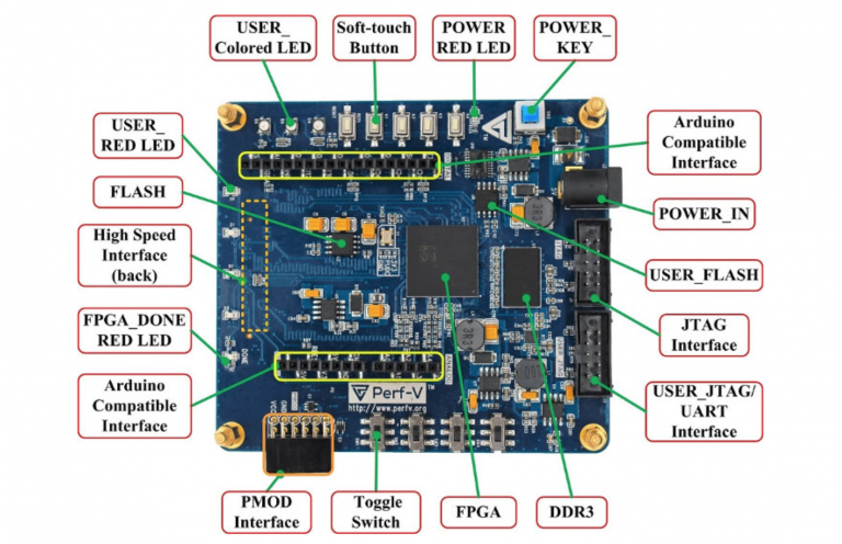
FII-PRX100 RISC-V development board
Suitable for FPGA study and training
Fully support FIE310 CPU running and system development
Suitable for user customized RV32G verification and validation
JTAG interface for FPGA and FIE310 CPU download and debug
Support Windows software and linux development environment
GCC compilation toolchain and graphical software development environment
Hardware resource: Switchs, Push Button ,USB to UART convertor, QSPI flash, I2CEEPROM, 100M/1G ethernet,USB keyboard mouse,GPIO, hdmi transmitter and camera etc.
1.System Design Objective
The main purpose of this system design is to complete FPGA learning, development and experiment with Xilinx-Vivado. The main device uses the Xilinx-XC7A100T-2FGG676I and is currently the latest generation of FPGA devices from Xilinx. The main learning and development projects can be completed as follows:
Basic FPGA design training
Construction and training of the SOPC (Microblaze) system
IC design and verification, the system provides hardware design, simulation and verification of RISC-V CPU
Development and application based on RISC-V
The system is specifically optimized for hardware design for RISC-V system applications.
2.System Resource
Extended memory
Use two Super Srams in parallel to form a 32-bit data interface with a maximum access space of 1M bytes.
Integrated FPGA Jtag and Risc-V Jtag by using single USB port.
Built-in RISC-V IPCore
CPU software debugger, no external RISC-V JTAG emulator required
12-pin GPIO connectors, in line with PMOD interface compatible.
4 Software Development System
Vivado 18.1 and later version for FPGA development, Microblaze SOPC
Freedom Studio-Win_x86_64 Software development for RISC-V CPU
5. Supporting Resources
RISC-V JTAG Debugger
Xilinx Altera JTAG Download Debugger
FII-PRX100 Development Guide
What is RISC-V Foundation?
RISC-V is a free and open ISA enabling a new era of processor innovation through open standard collaboration.
The RISC- V Foundation is a non-profit entity serving members and the industry and was originally developed in the Computer Science Division of the EECS Department at the University of California, Berkeley.
Recently RISC-V and GigaDevice announced the GD32V Series, which is said to be the world’s first 32-bit general-purpose microcontroller based on the RISC-V core.
It uses Xilinx Artix-7 FPGA, Vivado software development,and is designed for the RISC-V open source community and FPGA learning enthusiasts design development board.
It Integrates a variety of peripheral chips to provide a rich set of peripheral interfaces, including PMOD, Arduino, JTAG, UART interfaces, and high-speed interfaces for expansion of HDMI, VGA, USB2.0/3.0, camera, Bluetooth, expansion boards, etc. Strong flexibility.
Based on Perf-V’s self-developed smart car, it can use mobile phone Bluetooth to control the movement of the car, and can realize automatic tracing and obstacle avoidance functions.
You can also choose another one with the chip XC7A100T-1FTG256C, which has more logic cells and CLBs.
What is the next board are you expecting? Please feel to let us know in the forum: New Product Ideas. We will carefully listen to and take action!
A field-programmable gate array (FPGA) is an integrated circuit designed to be configured by a customer or a designer after manufacturing – hence the term “field-programmable”.
The FPGA configuration is generally specified using a hardware description language (HDL), similar to that used for an Application-Specific Integrated Circuit (ASIC). Circuit diagrams were previously used to specify the configuration, but this is increasingly rare due to the advent of electronic design automation tools.
pocket FPGA study Boards
FII was founded on making FPGA technology more approachable for students or FPGA beginners to learn. We partnered with the world leader and founder of modern day FPGA technology, Altera and Xilinx, to create platforms that were ideally suited for learning.
Below are boards that we recommend for beginning users. These boards have course material, books, and tutorials to get you started!
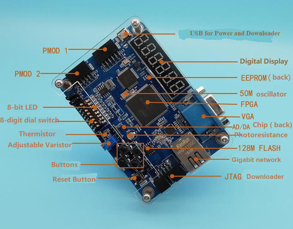
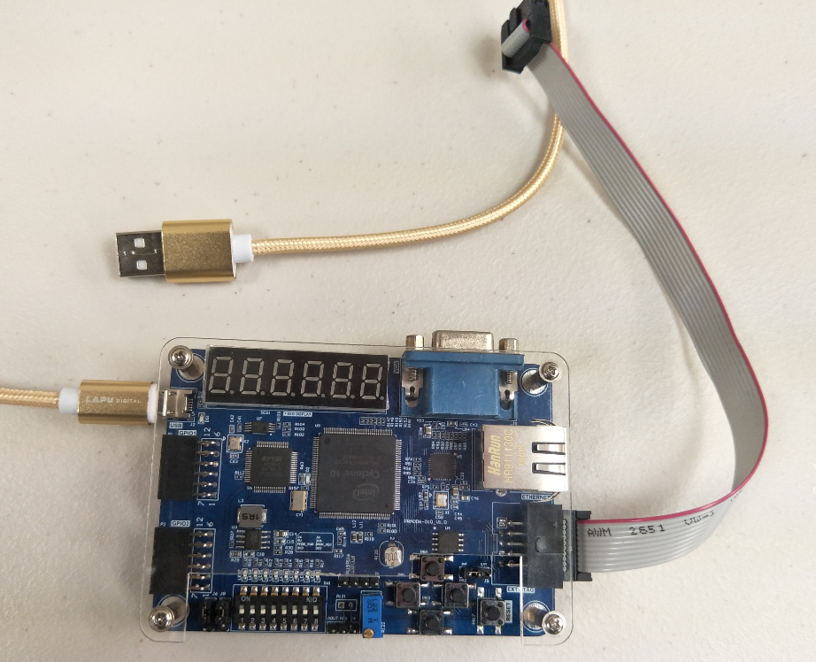
Micro usb Interface(Power Supply and downlaod ) × 1
SPI Communication Interface × 1
AD/DA Conversion chip × 1
JTAG Download Interface × 1
FLASH 32Mbit × 1
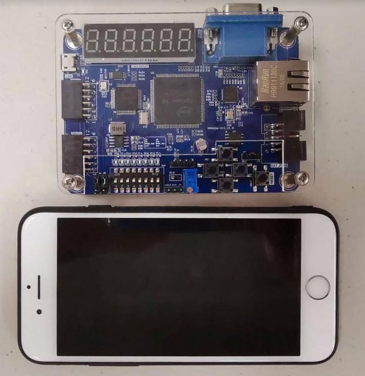
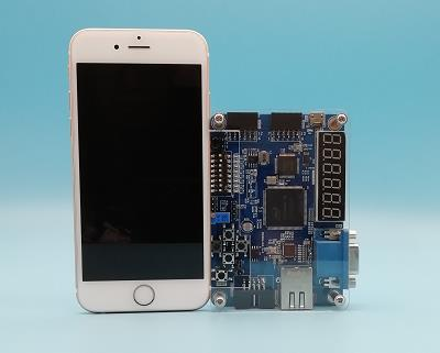
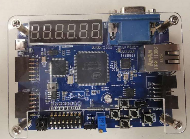
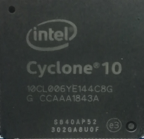
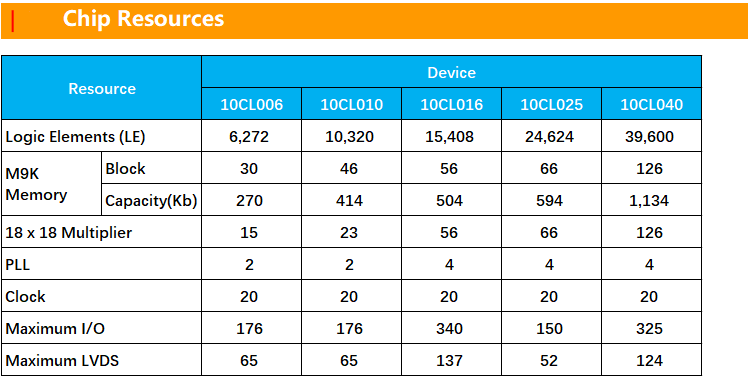
Chip ResourcesFPGA Study Board
The Biggest Hardware Benefits:
USB port for power supply, downloader, communications ;
One 50M Oscillator. A stable clock for development board;
6-digit common anode digital tube,display the data by dynamic scan;
1 VGA port to display picture and video;
1 I2C port EEPROM chip,Model: AT24C02;
1 adaptive 10M, 100M/1000M Ethernet port;
5 buttons,4 for programmable buttons , and one button for resetting;
1 Photoresistance. It can be used for simulating light control;
1 thermistor. It can be used for collecting temperature or simulating alarm function
An adjustable resistor can simulate voltage changes, etc.
1 PCF8591 AD/DA Conversion chip;
8-digit dial switch;
8-bit LED light-emitting diode;
One 128Mbit Flash Chip;
2 GPIO external port for communication extension port ;
One JTAGPort , and make PRA006/010 a functional JTAG down-loader, can be used as a JTAG downloader for Intel,Xilinx and other FPGA downloadable program;
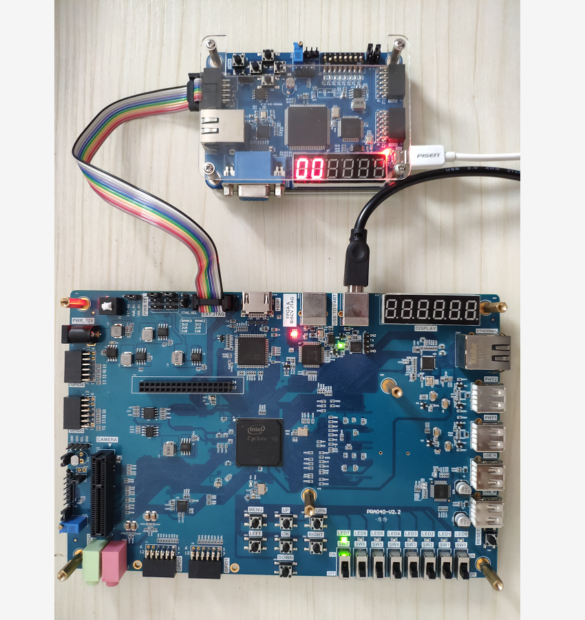
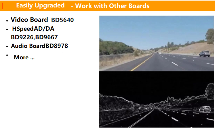
It can also be used with other FPGA development Boards:
FPGA for Beginner Boards Work Together with other BoardsEasily Work With Other Boards
FPGA Board For Beginner with free Experimental ManualsFPGA Board For Beginner with free Experimental Manuals and embeded Jtag downloaderBuy FPGA Boards
FPGAs provide benefits to designers of many types of electronic equipment, ranging from IOT, smart homes, smart energy grids, aircraft navigation, automotive driver’s assistance, medical ultrasounds and data center search engines, and so on.
We will send you experimental manuals when you have bought our pocket study board. PRA006 or PRA010
What is FPGA?
FPGA stands for “Field Programmable Gate Array“. As you may already know, FPGA essentially is a huge array of gates which can be programmed and reconfigured any time anywhere. “Huge array of gates” is an oversimplified description of FPGA. FPGA is indeed much more complex than a simple array of gates.
Some FPGAs has built-in hard blocks such as Memory controllers, high-speed communication interfaces, PCIe Endpoints, etc. But the point is, there are a lot of gates inside the FPGA which can be arbitrarily connected together to make a circuit of your choice. More or less like connecting individual logic gate ICs (again oversimplified but a good mental picture nonetheless).
FPGAs are manufactured by companies like Xilinx, Altera, Microsemi, etc… FPGAs are fundamentally similar to CPLDs but CPLDs are very small in size and capability compared to FPGAs.
What are the applications of FPGA?
Architecturally FPGAs are essentially a sea of gates which can be reconfigured to build almost any digital circuit that one can imagine.
This great flexibility along with the ability to reconfigure the device with different designs at-will makes FPGA a better choice compared to ASICs (Application Specific Integrated Circuit) for a lot of applications. For example, deep learning, AI or application acceleration system can re-program a single FPGA with different algorithms at different times to achieve the best performance. An ASIC would not be as flexible in such situations.
In certain applications, the number of individual units manufactured would be very small. Designing and manufacturing ASICs for these applications can be prohibitively expensive. In such situations, FPGA can offer very cost effective but robust solutions. The module form-factor boards such as the Narvi Spartan 7 FPGA Module make it easier to implement the applications without requiring end-product designers to take care of complex details such as FPGA power supplies, DDR3 routing, etc. Below are some of the potential applications of FPGAs in no particular order.
Cryptography
ASIC prototyping
Industrial, medical and Scientific Instruments
Audio/Video and Image processing and broadcasting
High-performance computing, AI, and Deep Learning
Military and Space applications
Networking, packet processing, and other communications
What is FPGA programming?
FPGA programming or FPGA development process is the process of planning, designing and implementing a solution on FPGA. The amount and type of planning vary from application to application. But creating a requirements document that captures all specific requirements and creating a design document that explains how the proposed solution would be implemented can be very helpful to enumerate potential problems and plan around them. A little bit of time spent creating a quality design document will save tons of time in refactoring, debugging and bug fixing later. Implementing a solution on FPGA includes building the design using one of the design entry methods such as schematics or HDL code such as Verilog or VHDL, Synthesizing the design (Synthesis, netlist generation, place and route etc..) in to output files that FPGAs can understand and program the output file to the physical FPGA device using programming tools. Entering the design using schematics is not used in the industry widely anymore. So we will keep the discussion limited to design entry using HDL (Hardware Description Language), specifically Verilog in this article series. Synthesis and programming are almost completely taken care of the vendor tools such as ISE and Vivado and Numato Lab configuration tools. All necessary steps to be taken by the user as part of design entry, synthesis and programming will be explained in subsequent sections.
The Benefits of FPGA
Flexibility
FPGA functionality can change upon every power-up of the device. So, when a design engineer wants to make a change, they can simply download a new configuration file into the device and try out the change.
Often, changes can be made to the FPGA without making costly PC board changes.
ASSPs and ASICs have fixed hardware functionality that can’t be changed without great cost and time.
Acceleration
FPGAs are sold “off the shelf” vs. ASICs (which require manufacturing cycles taking many months).
Because of FPGA flexibility, OEMs can ship systems as soon as the design is working and tested.
FPGAs provide off-load and acceleration functions to CPUs, effectively speeding up the entire system performance.
Integration
Today’s FPGAs include on-die processors, transceiver I/O’s at 28 Gbps (or faster), RAM blocks, DSP engines, and more. More functions within the FPGA mean fewer devices on the circuit board, increasing reliability by reducing the number of device failures.
Total Cost of Ownership (TCO)
While ASICs may cost less per unit than an equivalent FPGA, building them requires a non-recurring expense (NRE), expensive software tools, specialized design teams, and long manufacturing cycles.
Intel FPGAs support long lifecycles (15-years or more), avoiding the cost of redesigning and requalifying OEM production equipment if one of the electronic devices on-board goes end of life (EOL).
FPGAs reduce risk, allowing prototype systems to ship to customers for field trials, while still providing the ability to make changes quickly before ramping to volume production.
The concept behind an FPGA’s programmability is a basic building block containing various logic types that are connected and interconnected to perform any logic function. “Basic building block” is a generic term that I’m using, but you may hear terms like “logic cells,” “combinational logic blocks” (CLBs), or “logic array blocks” (LABs); it depends on the manufacturer. The basic building block contains logic resources and is the starting point that the FPGA uses to constructs the design.