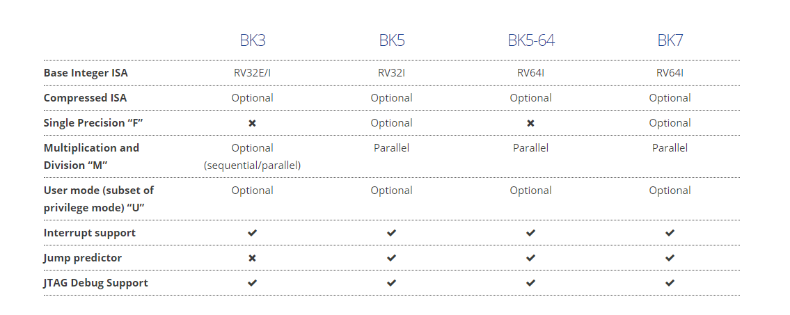
Codasip’s RISC-V-based processors (Bk) make use of the rich ecosystem of software and hardware enabled by the extensible, RISC-V Instruction-Set Architecture (ISA) Standard, while retaining the incredible flexibility of all Codasip-made cores.
Codasip currently offers the following base versions of the RISC-V architecture: with a 3-stage, 5-stage, and a 7-stage pipeline. All are fully compliant with the RISC-V specification and fully customizable.
In addition to the base processor implementation, Codasip provides standard support for optional instruction layers as defined by the current RISC-V specification.
ll Codasip Bk cores are fully customizable to the needs of your design. Changes can be made by Codasip as part of the standard deliverable, or by your own developers using our unique IP Generation Toolkit (Codasip Studio).
Need a single-cycle MAC, specialized crypto functions, or support for non-standard data types? No problem. Better yet, thanks to the extensible nature of the RISC-V ISA, all tailored cores remain RISC-V compliant, allowing you to use the growing SW Ecosystem.
STATE-OF-THE-ART COMMERCIAL SDK SUPPORT
The Bk cores are supported by industry-leading SDK that is based on LLVM, GNU and other open standards, but is optimized for your unique processor configuration and backed by Codasip’s comprehensive support.
OPEN, EXTENSIBLE, INDUSTRY-SUPPORTED
Codasip is proud to be a founding member of the RISC-V Foundation, joining industry leaders such as Google, Oracle, HP, AMD, Nvidia, and many others.
The power of RISC-V board is that it defines an ISA that helps a healthy HW and SW ecosystems develop, allowing each vendor to deliver their own unique value.
Modern FPGAs can speed up a wide range of applications, but they still require a lot of expertise. Intel aims to make it easier for the rest of the world to use programmable logic for server acceleration.
When it comes to speeding up computationally intensive workloads, GPUs are not the only game in town. FPGAs (field-programmable gate arrays) are also gaining traction in data centers.
While companies used to have to justify everything they wanted to migrate to the cloud, that scenario has flipped in recent years. Here’s how to make the best decisions about cloud computing.
These programmable logic devices, which can be reconfigured “in the field” for different tasks after manufacturing, have long been used in telecom gear, industrial systems, automotive, and military and aerospace applications. But modern FPGAs with large gate arrays, memory blocks, and fast IO are suitable for a wide range of tasks.
Microsoft has been using Altera FPGAs in its servers to run many of the neural networks behind services such as Bing searches, Cortana speech recognition, and natural-language translation. At the Hot Chips conference in August, Microsoft announced Project Brainwave, which will make FPGAs available as an Azure service for inferencing. Baidu is also working on FPGAs in its data center and AWS already offers EC2 F1 instances with Xilinx Virtex UltraScale+ FPGAs.
Most customers buy FPGAs as chips, and then design their own hardware and program them in a hardware description language such as VHDL or Verilog. Over time, some FPGAs have morphed into SoCs with ARM CPUs, hard blocks for memory and IO, and more (this week Xilinx just announced a family of Zync UltraScale+ FPGAs with a quad-core Cortex-A53 and the RF data converters for 5G wireless and cable). But the fact remains that FPGAs require considerable hardware and software engineering resources.
“One of the strengths of FPGAs is that they are infinitely flexible, but it is also one of their biggest challenges,” said Nicola Tan, senior marketing manager for data center solutions in Intel’s Programmable Solutions Group.
Now Intel is aiming to make it easier for other businesses to use FPGAs as server accelerators. This week the chipmaker announced the first of a new family of standard Programmable Acceleration Cards (PACs) for Xeon servers as well as software that makes them easier to program. In addition, Intel and partners are building functions for a wide variety of applications including encryption, compression, network packet processing, database acceleration, video streaming analytics, genomics, finance, and, of course, machine learning.
The PAC is a standard PCI Express Gen3 expansion card that can be plugged into any server. The first card combines the Arria 10 GX, a mid-range FPGA manufactured on TSMC’s 20nm process, with 8GB of DDR4 memory and 128MB of flash. It is currently sampling and will ship in the first half of 2018. Intel said it will also offer a PAC with the high-end Stratix 10, manufactured on its own 14nm process, but it hasn’t said when that version will be available.
Today’s successful organizations are quickly realizing that small-group collaboration allows them to innovate and create in ways that can deliver a significant competitive advantage. As a result, huddle rooms are growing increasingly popular in corporate campuses and small businesses.
Learn more about how huddle rooms can result in richer interactions, more productive meetings, stronger outcomes and a clear return on investment.
At Hot Chips in August, Microsoft provided a sneak preview of the kind of performance that the Stratix 10 can deliver in the data center and said it expects a production-level chip running at 500MHz with tuned software will deliver a whopping 90 teraops (trillions of operations per second) for AI inferencing using its custom data format.
In addition to the PACs, Intel will also offer an MCP (multi-chip package) that combines a Skylake Xeon Scalable Processor and an FPGA. This is something Intel has been talking up since the $16.7 billion acquisition of Altera, and it has previously shown test chips with Broadwell Xeons and FPGAs, but the first commercial chip will arrive in the second half of 2018.
Conceptually, this isn’t really all that different from the Altera and Xilinx SoCs that already include ARM CPUs, but x86 processors should deliver higher performance and Intel can leverage the proprietary interconnect and 2.5D packaging technologies it has been developing.
RTL stands for Register Transfer Level. You might also encounter the terms Register Transfer Logic or Register Transfer Language, they all mean the same in the context of hardware designing. RTL is a higher level abstraction for your digital hardware design and comes somewhere between strictly behavioral modeling on one end and purely gate-level structural modeling on other ends.
Behavioral modeling is explained in the next articles in this series so don’t be daunted with this term. Gate modeling means describing hardware using basic gates which is quite tedious. RTL can also be thought of as analogous to the term “pseudo-code” used in software programming. It is possible to describe the hardware design as sequences of steps (or flow) of data from one set of registers to next at each clock cycle.
Therefore, RTL is also commonly referred to as “dataflow” design. Once the RTL design is ready, it is easier to convert it into actual HDL code using languages such as Verilog, VHDL, SystemVerilog or any other hardware description language. HDL and Verilog are explained in the next section. Check out the Wikipedia page on RTL for more information (https://en.wikipedia.org/wiki/Register-transfer_level)
What is Verilog?
In the previous paragraphs, I mentioned the word “oversimplified” two times. The reason is that FPGAs are much much more than just a bunch of gates. While it is possible to build logic circuits of any complexity simply by arranging and connecting logic gates, it is just not practical and efficient. So we need a way to express the logic in some easy to use format that can be converted to an array of gates eventually.
Two popular ways to accomplish this are schematic entry and HDLs (Hardware Description Language). Before HDLs were popular, engineers used to design everything with schematics. Schematics are wonderfully easy for small designs but are painfully unmanageable for a large design (think about Intel engineers drawing schematics for Pentium, which has millions of gates! it is unacceptably complex).
If you have some electronics background, your initial tendency will be to use schematics to realize your design instead of learning a new language (This happened to me, honestly). For the aforementioned reasons, we will stick with HDL throughout this tutorial.
Verilog is a Hardware Description Language (HDL) which can be used to describe digital circuits in a textual manner. We will write our design for FPGA using Verilog (as if you write microcontroller programs in C and Assembly). Learning Verilog is not that hard if you have some programming background. VHDL is also another popular HDL used in the industry extensively.
Verilog and VHDL share more or less same market popularity, but I chose Verilog since it is easy to learn and its syntactical similarity to C language. Once you are comfortable with Verilog, it should be easy learning VHDL as well. Want to read more about Verilog? Check out this wiki page (http://en.wikipedia.org/wiki/Verilog) or check this tutorial (http://www.asic-world.com/verilog/index.html).
What tools do we need?
1. A good text editor (I use Notepad++ )
2. Xilinx ISE Webpack (Download from Xilinx for free. Registration required).
FPGA Beginner Boards
3. A good FPGA development board (Mimas V2 FPGA Development Board is used in the examples here. Picture of Mimas V2 is shown at the top of this page. If you have an Elbert V2 Spartan 3A FPGA board, that should work perfectly too. There are some differences when setting up the project for Mimas V2 vs Elbert V2 but I will point them out when it is necessary.)
4. Mimas V2 or Elbert V2 Configuration downloader software (Required only if Mimas V2 /Elbert V2 FPGA Development Board is used. Download from the respective product pages)
Additional tools may be necessary to follow advanced topics in this series. Information about such tools will be shared ass they are needed.
RISC-V is a free and open ISA enabling a new era of processor innovation through open standard collaboration.
FII-PRX100 Risc-V FPGA Board is a ready-to-use development platform designed around the Field Programmable Gate Array (FPGA) from Xilinx. It was designed to cover all aspects of FPGA Development and Experiment, RISC-V SOC . The main application areas aim at smart home, Wearable, sensor Fusion, IOT, and industrial control etc.
FII-PRX100 Risc-V FPGA Board is a ready-to-use development platform designed around the Field Programmable Gate Array (FPGA) from Xilinx. It was designed to cover all aspects of FPGA Development and Experiment, RISC-V SOC . The main application areas aim at smart home, Wearable, sensor Fusion, IOT, and industrial control etc.
FII-PRA040 RiscV Educational Platform is a ready-to-use development platform designed around the Field Programmable Gate Array (FPGA) from Intel Altera. RISC-V (pronounced “risk-five”) is an open-source hardware instruction set architecture (ISA) based on established reduced instruction set computer (RISC) principles.
The RISC- V Foundation is a non-profit entity serving members and the industry and was originally developed in the Computer Science Division of the EECS Department at the University of California, Berkeley.
Recently RISC-V and GigaDevice announced the GD32V Series, which is said to be the world’s first 32-bit general-purpose microcontroller based on the RISC-V core.
Today we released Longan Nano development board powered by GD32VF103CBT6 MCU today and it only costs $4.90.
Sipeed Longan Nano is a development board based on GD32VF103CBT6 MCU with RISC-V 32-bit core of GigaDevice.
It is convenient for students, engineers and geek enthusiasts to contact the new-generation RISC-V processor.
Longan Nano comes with a 0.96inch 160×80 IPS RGB LCD and an acrylic transparent case.
Besides Longan Nano, let’s through back to take a look at what happened about RISC -V at Seeed Studio in 2019. Please don’t forget our full selection of Sipeed products, which will help you a lot to getting started with AI projects in a cost-effective way.
February – $7.9 RISC-V Module – Sipeed MAIX-I module w/o WiFi ( 1st RISC-V 64 AI Module, K210 inside)
MAIX is Sipeed’s purpose-built module designed to run AI at the edge, we called it AIoT. It delivers high performance in a small physical and power footprint, enabling the deployment of high-accuracy AI at the edge, and the competitive price make it possible embed to any IoT devices. As you see, Sipeed MAIX is quite like Google edge TPU, but it act as master controller, not an accelerator like edge TPU, so it is more low cost and low power than AP+edge TPU solution.
RISC-V is the new hotness, and companies are churning out code and announcements. Eventually, RISC-V microcontrollers and SoCs will cost just a few bucks. This day might be here, with Seeed’s Sipeed MAix modules. it’s a RISC-V chip you can buy right now, the bare module costs eight US dollars, there are several modules, and it has “AI.”
March – Grove AI HAT for Edge Computing
Next, in March, we released Grove AI HAT.
The Grove AI HAT for Edge Computing is built around Sipeed MAix M1 AI MODULE with Kendryte K210 processor inside. It’s a low cost but powerful raspberry pi AI hat which assists raspberry pi run the AI at the edge, it also can work independently for edge computing applications.
The MAix M1 is a powerful RISC-V 600MHz AI module that features dual-core 64-bit CPU, 230GMULps 16-bit KPU(Neural Network Processor), FPU(Float Point Unit) supports DP&SP, and APU(Audio Processor) supports 8 mics. In addition to the powerful Kendryte K210 processor, the Grove AI HAT for Edge Computing board provides a wealth of peripherals: I2C/UART/SPI/I2S/PWM/GPIO. The HAT also offers an LCD and a camera interface, which supports the Sipeed 2.4inch QVGA LCD and DVP camera, it will be helpful and convenience with your AI vision project.
It’s a low cost but powerful raspberry pi AI hat which assists raspberry pi run the AI at the edge, it also can work independently for edge computing applications. The MAix M1 is a powerful RISC-V 600MHz AI module that features dual-core 64-bit CPU, 230GMULps 16-bit KPU(Neural Network Processor), FPU(Float Point Unit) supports DP&SP, and APU(Audio Processor) supports 8 mics. In addition to the powerful Kendryte K210 processor, the Grove AI HAT for Edge Computing board provides a wealth of peripherals: I2C/UART/SPI/I2S/PWM/GPIO. The hat also offers an LCD and a camera interface, which supports the Sipeed 2.4inch QVGA LCD and DVP camera, it will be helpful and convenience with your AI vision project.
Based on MAIX Module, the Maixduino is a RISC-V 64 development board for AI + IoT applications. Different from other Sipeed MAIX dev. boards, Maixduino was designed in an Arduino Uno form factor, with ESP32 module on board together with MAIX AI module.
Maixduino will help you extend AI function in the following applications:
Smart Home applications like robot cleaners, smart speakers, electronic door locks, household monitoring etc.
Medical Industry applications like Auxiliary diagnosis and treatment, medical image recognition, emergency alarm etc.
Smart Industry applications like industrial machinery, intelligent sorting, monitoring of electrical equipment, etc.
Education applications like educational robots, intelligent interactive platforms, educational efficiency inspection, etc.
Agriculture applications like agricultural monitoring, pest and disease monitoring, automated control, etc.
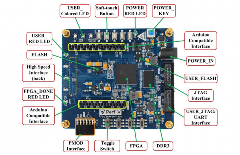
Perf-V is a FPGA demo board designed for RISC-V opensource community by PerfXLab. It integrates various peripheral chips and offers many interfaces.
It uses Xilinx Artix-7 FPGA, Vivado software development,and is designed for the RISC-V open source community and FPGA learning enthusiasts design development board.
It Integrates a variety of peripheral chips to provide a rich set of peripheral interfaces, including PMOD, Arduino, JTAG, UART interfaces, and high-speed interfaces for expansion of HDMI, VGA, USB2.0/3.0, camera, Bluetooth, expansion boards, etc. Strong flexibility.
Based on Perf-V’s self-developed smart car, it can use mobile phone Bluetooth to control the movement of the car, and can realize automatic tracing and obstacle avoidance functions.
You can also choose another one with the chip XC7A100T-1FTG256C, which has more logic cells and CLBs.
What is the next board are you expecting? Please feel to let us know in the forum: New Product Ideas. We will carefully listen to and take action!