What is RTL and Verilog ?

What is RTL?

RTL stands for Register Transfer Level. You might also encounter the terms Register Transfer Logic or Register Transfer Language, they all mean the same in the context of hardware designing. RTL is a higher level abstraction for your digital hardware design and comes somewhere between strictly behavioral modeling on one end and purely gate-level structural modeling on other ends.

Behavioral modeling is explained in the next articles in this series so don’t be daunted with this term. Gate modeling means describing hardware using basic gates which is quite tedious. RTL can also be thought of as analogous to the term “pseudo-code” used in software programming. It is possible to describe the hardware design as sequences of steps (or flow) of data from one set of registers to next at each clock cycle.

Therefore, RTL is also commonly referred to as “dataflow” design. Once the RTL design is ready, it is easier to convert it into actual HDL code using languages such as Verilog, VHDL, SystemVerilog or any other hardware description language. HDL and Verilog are explained in the next section. Check out the Wikipedia page on RTL for more information (https://en.wikipedia.org/wiki/Register-transfer_level)

What is Verilog?

In the previous paragraphs, I mentioned the word “oversimplified” two times. The reason is that FPGAs are much much more than just a bunch of gates. While it is possible to build logic circuits of any complexity simply by arranging and connecting logic gates, it is just not practical and efficient. So we need a way to express the logic in some easy to use format that can be converted to an array of gates eventually.

Two popular ways to accomplish this are schematic entry and HDLs (Hardware Description Language). Before HDLs were popular, engineers used to design everything with schematics. Schematics are wonderfully easy for small designs but are painfully unmanageable for a large design (think about Intel engineers drawing schematics for Pentium, which has millions of gates! it is unacceptably complex).

If you have some electronics background, your initial tendency will be to use schematics to realize your design instead of learning a new language (This happened to me, honestly). For the aforementioned reasons, we will stick with HDL throughout this tutorial.

Verilog is a Hardware Description Language (HDL) which can be used to describe digital circuits in a textual manner. We will write our design for FPGA using Verilog (as if you write microcontroller programs in C and Assembly). Learning Verilog is not that hard if you have some programming background. VHDL is also another popular HDL used in the industry extensively.

Verilog and VHDL share more or less same market popularity, but I chose Verilog since it is easy to learn and its syntactical similarity to C language. Once you are comfortable with Verilog, it should be easy learning VHDL as well. Want to read more about Verilog? Check out this wiki page (http://en.wikipedia.org/wiki/Verilog) or check this tutorial (http://www.asic-world.com/verilog/index.html).

What tools do we need?

1. A good text editor (I use Notepad++ )

2. Xilinx ISE Webpack (Download from Xilinx for free. Registration required).

FPGA Beginner Boards

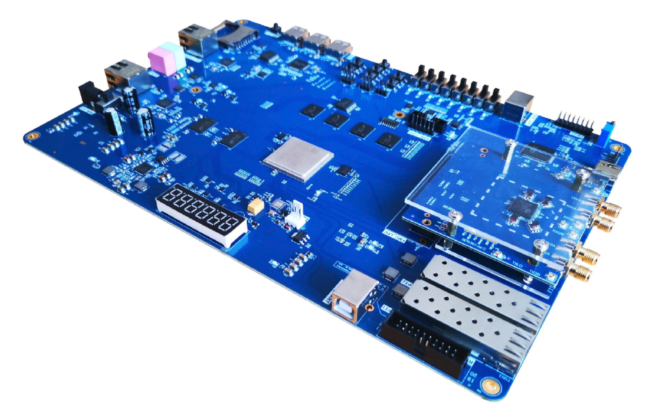
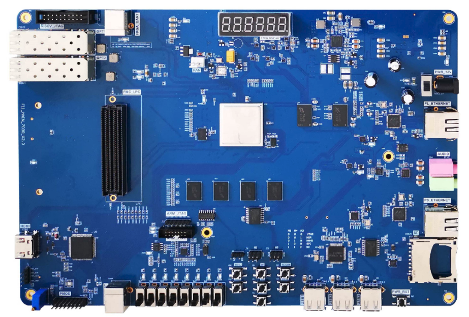
3. A good FPGA development board (Mimas V2 FPGA Development Board is used in the examples here. Picture of Mimas V2 is shown at the top of this page. If you have an Elbert V2 Spartan 3A FPGA board, that should work perfectly too. There are some differences when setting up the project for Mimas V2 vs Elbert V2 but I will point them out when it is necessary.)

4. Mimas V2 or Elbert V2 Configuration downloader software (Required only if Mimas V2 /Elbert V2 FPGA Development Board is used. Download from the respective product pages)

Additional tools may be necessary to follow advanced topics in this series. Information about such tools will be shared ass they are needed.

Altera Risc-V FPGA Board – FII-PRA040 risc-v SOPC AI Cyclone10

It was designed for use in all fields of FPGA development and experiments.

Communication

Digital Communication DSP(FPGA)

Network

100M/1G Interface,switch VLAN

USB:

USB2.0 Engine Development

CPU:

RISC-V CPU 32bit Ecosystem Dvelopment and Educational Experiments

Artificial Intelligence

Voice collection, speech recognition Image acquisition and image recognition, deep learning

Features

10CL040 10CL080
Logic elements (LEs) (K) 40 80
Memory blocks(9K) 126 305
LMemory block(Kb) 1134 2745
18×18 multipliers 126 244
Phase-locked loop(PLL) 4 4
Global clock networks 20 20

System Features:

    • Sram IS61WV25616 (2 pieces ) 256K x 32bit
    • Spi serial flash (16M bytes)
    • JTAG:  two jtag programmable interfaces
    • power Supply: 12V adapter source

System Connectivity

  1. 10/100/1000 Mbps Ethernet
  2. Hdmi: Hdmi out (1920×1080@60Hz)
  3. USB to Serial Interface:USB-UART bridge


Interaction and Sensory Devices

  1. 8 Switches
  2. 7 Buttons (up , down, left, right, ok, menu, return)
  3. 1 Reset button
  4. 8 LEDs
  5. 1 4-digit 7 segment display
  6. 1 I2c interface (24c02 eeprom)
  7. High resolution graphic LCD interface
  8. Image input interface

Expansion Connectors

    • 4 gpio connectors (compatible with digilent Pmod)

Features and Benefits

  1. gpio  (16 ) 2×8 standard 2.54mm connectors (pin)
  2. led  outport (8 个) 0603 smd
  3. switch (8 in one group) smd 
  4. 7 Buttons (up , down, left, right, ok, menu, return)
  5. i2c  24c02 smd soic
  6. spi  flash MX25L6433F 8-SOP (8M bytes)
  7. usb2uart ft2232C/H (2 uart ) Or cp2102 (1  uart)
  8. jtag 2×5 standard 2.54mm connectors(pin)
  9. eth  1G CAT5 Ethernet (rtl8111e)
  10. Digital tube 7seg (4) oasistek TOF-5421BMRL-N
  11. Hdmi out adv7511hdmi_adv7511.SchDoc
  12. Test Port1×6 Standard 2.54mm connector (pin)

After nearly a decade of neglect, the last year has seen a big uptick in the adoption of the the RISC-V standard. The arrival of the first commercially-available open source system-on-chip (SoC) based on the architecture — the 32-bit Freedom Everywhere 310 — along with the first Arduino-compatible development board called the HiFive1, from the Bay Area startup SiFive, was seen as a real milestone by the open hardware community.

Which doesn’t mean that keeping other independent implementations of the standard around isn’t still important, which is where DarkRISCV comes in.

While the DarkRISCV implementation is not as full featured as some other RISC-V implementations, it does implement most of the RISC-V RV32I instruction set and works on real Spartan-6 hardware.

With the first GAP8 processor samples by Open-Silicon shipping, we’re almost in a place where we have multiple vendors producing open silicon built around the RISC-V core, and when that happens we’ll be in a very different place. At that point, we’re in a real open hardware environment because we no longer have vendor lock in, and it’s going to be interesting to see whether that makes a difference to the availability of boards based on RISC-V.

Until then, however, the availability of implementations of the RISC-V architecture, and the ability for people to get hands on with it—whether that’s using an FPGA or not—is important to the ecosystems continued health.

Full details of the DarkRISCV implementation, as well as some interesting notes with indications of not just what, and how, he implemented various parts of the standard, but also why Samsoniuk took certain paths are available in the project’s GitHub repo.

FPGA Development Board and Educational Platform ( xc7z030 ZYNQ EVB Board )

FII-PE7030 is a ready-to-use for educational platform which has been designed to cover FPGA development and experiment, ARM SOC development and experiment, network(copper or fiber) development ,digital communication and SDR(software define radio) with daughter board FII-BD9361 plug on.

Basic Experiment Functions:

FII-PE7030  xc7z030 zynq evb board  is a ready-to-use for educational platform which has been designed to cover FPGA development and experiment,  ARM SOC development and experiment,  network(copper or fiber) development ,digital communication and SDR(software define radio) with daughter board FII-BD9361 plug on.  It was designed for university students, teachers, and all other industrail professionals.  FII-PE7030 is an incredibly flexible processing platform, capable of adapting to most of your project requires.

More surprising show up that recently Engineers has successful port RISC-V(RV32G) and RV64I to this platform, it becomes a real RISC-V SOC platform.

Application:

wireless Communication
DBC(digital base band communication) and DSP
SDR Software defined radio
LTE protocol analysis
4/5G  base station

Network communication:
100M/1G  ethernet communication both for PS and PL
10G SFP+  fibre communication with multiple protocol supported like LAN, SONET/SDH, CPRI etc.
Network switch and router
VLAN
Spanning  Tree

USB:
1 480M high speed USB2.0  HUB
4 480M high speed USB2.0  connectors

CPU:
RISC-V CPU 32bit ecosystem development ,verification and validation
RISC-V CPU 64bit ecosystem development,verification and validation

Artificial Intelligence:
Audio or Voice Collection, Speech Recognition
Image Acquisition and Image Recognition, Deep Learning

IOT: ALL kinds of IOTs with RISC-V system

FII-PE7030 System Hardware Resources:

  1. 2 ports 10G Ethernet(Fibre)
  2. 2 ports100M/1G Ethernet, one for PS and for PL
  3. 1 HDMI output Interface。
  4. dual channel Audio Interface
  5. AD9361 Interface(FMC-LPC)
  6. 8 LEDs
  7. 8 switches
  8. 8 buttons
  9. GPIO Expansion Port
  10. JTAG Debug Interface
  11. 1GB ddr3 –SOC(PS)
  12. 1GB ddr3—FPGA(PL)
  13. SDCARD Interface
  14. 32M Serial FLASH
  15. Serial EEPROM
  16. 12bit 1MPS ADC
  17. Temperature Sensor