500M Camera module ov5640

OmniVision’s OV5645 is a high performance, 5-megapixel system-on-chip (SOC) ideally suited for the cost-sensitive segment of the mobile handset market. The CameraChip™ sensor’s single MIPI port replaces both a bandwidth-limited DVP interface and a costly embedded JPEG compressor, allowing the new OV5645 sensor to save significant silicon area and cost. An embedded autofocus control with voice coil motor driver offers further cost savings for the end user, making the OV5645 a highly attractive alternative to other 5-megapixel sensors currently on the market.

The OV5645 also features a new picture-in-picture (PIP) architecture that offers an easy-to- implement, low-cost dual camera system solution for mobile handsets and smartphones. The feature is based on a master/slave configuration where a front-facing camera (OV7965) can be connected through the OV5645 master camera, enabling a two-camera system with PIP functionality without the need for an additional MIPI interface into the baseband processor.

Built on OmniVision’s 1.4-micron OmniBSI™+ pixel architecture, the OV5645 offers high performance 5-megapixel photography and 720p HD video at 60 frames per second (fps) and 1080p HD video at 30 fps with complete user control over formatting and output data transfer. The sensor’s 720p HD video is captured in full field-of-view with 2×2 binning, which doubles the sensitivity and improves the signal-to-noise ratio (SNR). A unique post-binning, re-sampling filter function removes zigzag artifacts around slant edges and minimizes spatial artifacts to deliver even sharper, crisper color images.

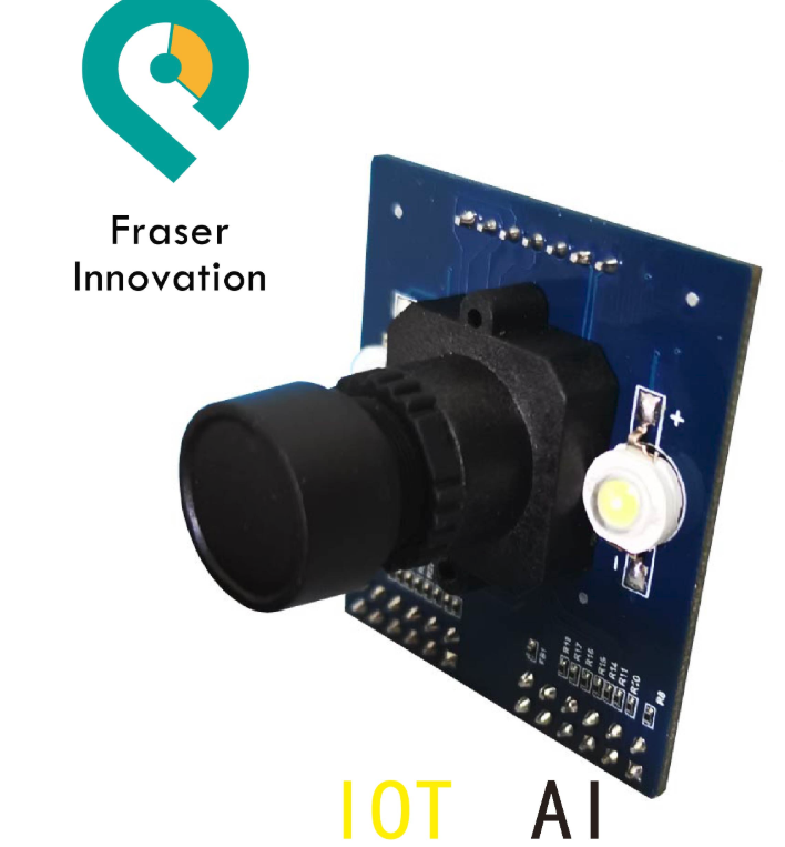
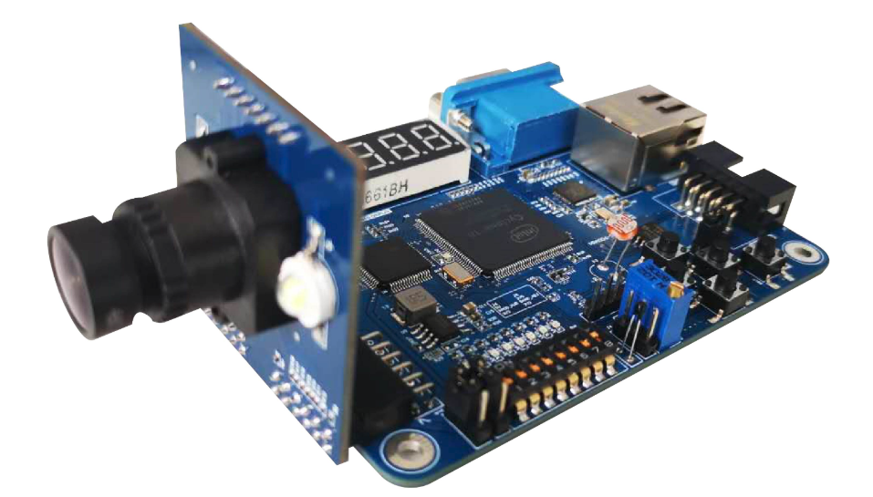
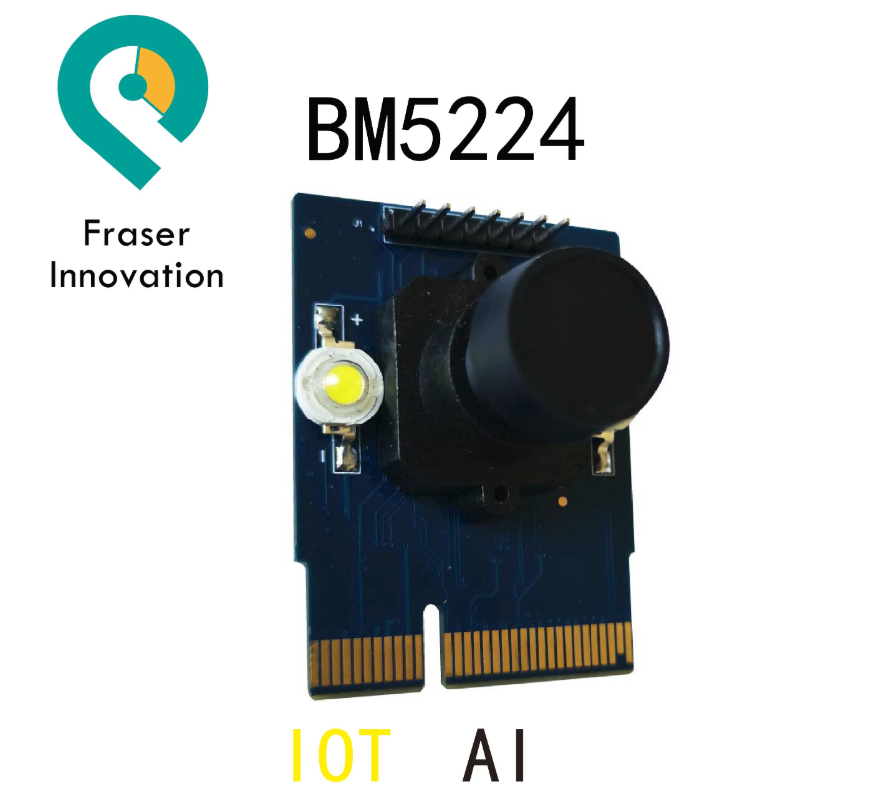
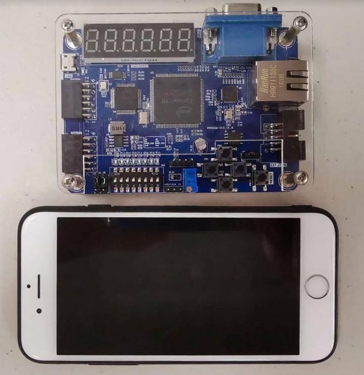
Fraser Innovation Inc develops BD5640 that contains a video camera based on video sensor OV5640 (CMOS). BD5640 support PMOD connector and it is compatible with different kinds of FII developing boards.

1.Introduction

The FII-BD5640-PMOD is a camera module designed to integrate the Omnivision ov5640 5 megapixel (MP) color image sensor , with its compatible power supply and oscillator. This board can be used with different kinds of FII FPGA development boards. Power supply for BD5640 is 3V3. The sensor includes lots of internal processing functions that can adjust white balance, saturation, hue, sharpness, and gamma correction.

The output data interface support general Digital output interface and dual-lane MIPI CSI-2 interface, so it can provides enough data bandwidth for common video streaming formats such as 1080p and 720p. The ov5640 (color) image sensor uses DVP data interface and SCCB control interface.

2.Basic Features

  1. 5MP color system-on-chip image sensor
  2. General digital output and Dual lane MIPI CSI-2 image sensor interface
  3. Supports QSXGA@15hz, 1080p@30Hz, 720p@60Hz,VGA@90Hz and QVGA@120Hz
  4. Output format include RAW10, RGB565, CCIR656, YUV422/420, YCbCr422, and JPEG compression
  5. M12 22mm lens mount with M12 3.6mm focus lens
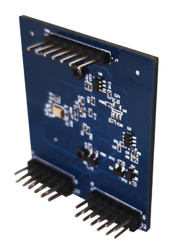
  6. Small PCB size for flexible designs (40mm*44mm)
  7. Powered up from double standard PMOD connector
  8. Supports FII-7030 and other FII FPGA development boards

4k 500M Camera Module – ov5640 – FII-BD5640 PCIE Interface

The OV5640 (color) image sensor is a low voltage, high-performance, 1/4-inch 5 megapixel CMOS image sensor that provides the full functionality of a single chip 5 megapixel (2592×1944) camera using OmniBSI™ technology in a small footprint package.

It provides full-frame, sub-sampled, windowed or arbitrarily scaled 8-bit/10-bit images in various formats via the control of the Serial Camera Control Bus (SCCB) interface.

The OV5640 has an image array capable of operating at up to 15 frames per second (fps) in 5 megapixel resolution with complete user control over image quality, formatting and output data transfer.

All required image processing functions, including exposure control, gamma, white balance, color saturation, hue control, defective pixel canceling, noise canceling, etc., are programmable through the SCCB interface or embedded microcontroller. The OV5640 also includes a compression engine for increased processing power.

In addition, Omnivision image sensors use proprietary sensor technology to improve image quality by reducing or eliminating common lighting/electrical sources of image contamination, such as fixed pattern noise, smearing, etc., to produce a clean, fully stable, color image.

OmniVision’s OV5645 is a high performance, 5-megapixel system-on-chip (SOC) ideally suited for the cost-sensitive segment of the mobile handset market. The CameraChip™ sensor’s single MIPI port replaces both a bandwidth-limited DVP interface and a costly embedded JPEG compressor, allowing the new OV5645 sensor to save significant silicon area and cost. An embedded autofocus control with voice coil motor driver offers further cost savings for the end user, making the OV5645 a highly attractive alternative to other 5-megapixel sensors currently on the market.

The OV5645 also features a new picture-in-picture (PIP) architecture that offers an easy-to- implement, low-cost dual camera system solution for mobile handsets and smartphones. The feature is based on a master/slave configuration where a front-facing camera (OV7965) can be connected through the OV5645 master camera, enabling a two-camera system with PIP functionality without the need for an additional MIPI interface into the baseband processor.

Built on OmniVision’s 1.4-micron OmniBSI™+ pixel architecture, the OV5645 offers high performance 5-megapixel photography and 720p HD video at 60 frames per second (fps) and 1080p HD video at 30 fps with complete user control over formatting and output data transfer. The sensor’s 720p HD video is captured in full field-of-view with 2×2 binning, which doubles the sensitivity and improves the signal-to-noise ratio (SNR). A unique post-binning, re-sampling filter function removes zigzag artifacts around slant edges and minimizes spatial artifacts to deliver even sharper, crisper color images.

Can FPGA board used in web hosting service ?

Intel pushes FPGAs into the data center

Modern FPGAs can speed up a wide range of applications, but they still require a lot of expertise. Intel aims to make it easier for the rest of the world to use programmable logic for server acceleration.

When it comes to speeding up computationally intensive workloads, GPUs are not the only game in town. FPGAs (field-programmable gate arrays) are also gaining traction in data centers.

While companies used to have to justify everything they wanted to migrate to the cloud, that scenario has flipped in recent years. Here’s how to make the best decisions about cloud computing.

These programmable logic devices, which can be reconfigured “in the field” for different tasks after manufacturing, have long been used in telecom gear, industrial systems, automotive, and military and aerospace applications. But modern FPGAs with large gate arrays, memory blocks, and fast IO are suitable for a wide range of tasks.

Microsoft has been using Altera FPGAs in its servers to run many of the neural networks behind services such as Bing searches, Cortana speech recognition, and natural-language translation. At the Hot Chips conference in August, Microsoft announced Project Brainwave, which will make FPGAs available as an Azure service for inferencing. Baidu is also working on FPGAs in its data center and AWS already offers EC2 F1 instances with Xilinx Virtex UltraScale+ FPGAs.

Most customers buy FPGAs as chips, and then design their own hardware and program them in a hardware description language such as VHDL or Verilog. Over time, some FPGAs have morphed into SoCs with ARM CPUs, hard blocks for memory and IO, and more (this week Xilinx just announced a family of Zync UltraScale+ FPGAs with a quad-core Cortex-A53 and the RF data converters for 5G wireless and cable). But the fact remains that FPGAs require considerable hardware and software engineering resources.

“One of the strengths of FPGAs is that they are infinitely flexible, but it is also one of their biggest challenges,” said Nicola Tan, senior marketing manager for data center solutions in Intel’s Programmable Solutions Group.

Now Intel is aiming to make it easier for other businesses to use FPGAs as server accelerators. This week the chipmaker announced the first of a new family of standard Programmable Acceleration Cards (PACs) for Xeon servers as well as software that makes them easier to program. In addition, Intel and partners are building functions for a wide variety of applications including encryption, compression, network packet processing, database acceleration, video streaming analytics, genomics, finance, and, of course, machine learning.

The PAC is a standard PCI Express Gen3 expansion card that can be plugged into any server. The first card combines the Arria 10 GX, a mid-range FPGA manufactured on TSMC’s 20nm process, with 8GB of DDR4 memory and 128MB of flash. It is currently sampling and will ship in the first half of 2018. Intel said it will also offer a PAC with the high-end Stratix 10, manufactured on its own 14nm process, but it hasn’t said when that version will be available.

At Hot Chips in August, Microsoft provided a sneak preview of the kind of performance that the Stratix 10 can deliver in the data center and said it expects a production-level chip running at 500MHz with tuned software will deliver a whopping 90 teraops (trillions of operations per second) for AI inferencing using its custom data format.

In addition to the PACs, Intel will also offer an MCP (multi-chip package) that combines a Skylake Xeon Scalable Processor and an FPGA. This is something Intel has been talking up since the $16.7 billion acquisition of Altera, and it has previously shown test chips with Broadwell Xeons and FPGAs, but the first commercial chip will arrive in the second half of 2018.

Conceptually, this isn’t really all that different from the Altera and Xilinx SoCs that already include ARM CPUs, but x86 processors should deliver higher performance and Intel can leverage the proprietary interconnect and 2.5D packaging technologies it has been developing.

How to learn Learning Verilog ?

Learning Verilog itself is not a difficult task, but creating a good design can be. But we focus on simple designs here and I will try my best to explain things as simple as possible.

If you had been programming with procedural languages such as C, C++, you will have to make up your mind to understand that not all things happen sequentially in the digital world. A lot of things happen parallel too. When I started learning Verilog, I used to write code sequentially as if I was writing a C program. C programs are running on microprocessors, which execute one instruction at a time sequentially. So it is easy to write a program in a way how you want things to happen one step at a time.

And if you look closely, this is the weak point of microprocessors / microcontrollers.

You need a fpga board to study verilog

They can do only one thing at a time, one and only one thing (of course I’m talking about single core devices!). But unlike microprocessors, digital circuits (FPGAs, CPLDs, and ASICs) can do many things at the same time. And you need to learn how to visualize many things happening at the same time in contrast to many things happening at different times, one thing at a time, in a procedural language.

Verilog Modules

A Verilog module is a design unit similar to a black-box, with a specific purpose as engineered by the RTL designer. It has inputs, outputs and it functions as per its intended design. A simplest Verilog module could be a simple NOT gate, as shown in the second image below, whose sole job is to invert the incoming input signal. There is no upper bound on the complexity of the Verilog modules, they can even describe complete processor cores! Verilog deals with digital circuits.

In Verilog realm, modules can be considered as equivalent to components in a digital circuit, as simple as a gate or a complex entity like ALU, counter, etc… Modules are analogous to classes in C++ in a way that it is self-contained and give a finite number of methods (ports) to interact with the external world.

Modules can be instantiated like classes are instantiated in C++ too. But beware; modules are not 100% similar to classes when it is implemented. For easy understanding, a module can be simply represented graphically as a box with a number of ports.

The ports can be inputs, outputs or bidirectional. Ports can be single bit or multiple bits in width. The image below represents a module with a few inputs and outputs. The number of inputs and outputs, their width and direction will depend solely on the functionality of the module.

Fundamentally Verilog (or most HDLs for that matter) is all about creating modules, interconnecting them and managing the timing of interactions.

Enough talk, we didn’t even write a “Hello World” program yet. So how do we get our hands dirty with Verilog? Let us design a NOT gate in Verilog, simulate it and test it in real hardware. A NOT gate (a.k.a an inverter) would be the simplest of all gates. The output of an inverter is always the negation of the input. ie; B = !A, where A is the input and B is the output. Below table summarize the behavior of NOT gate as a truth table.