AD9361 RF Transceiver Features

The AD9361 is a high performance, highly integrated radio frequency (RF) Agile Transceiver™ designed for use in 3G and 4G base station applications. Its programmability and wideband capability make it ideal for a broad range of transceiver applications.

The device combines a RF front end with a flexible mixed-signal baseband section and integrated frequency synthesizers, simplifying design-in by providing a configurable digital interface to a processor.

The AD9361 receiver LO operates from 70 MHz to 6.0 GHz and the transmitter LO operates from 47 MHz to 6.0 GHz range, covering most licensed and unlicensed bands. Channel bandwidths from less than 200 kHz to 56 MHz are supported.

The two independent direct conversion receivers have state-of-the-art noise figure and linearity. Each receive (RX) subsystem includes independent automatic gain control (AGC), dc offset correction, quadrature correction, and digital filtering, thereby eliminating the need for these functions in the digital baseband.

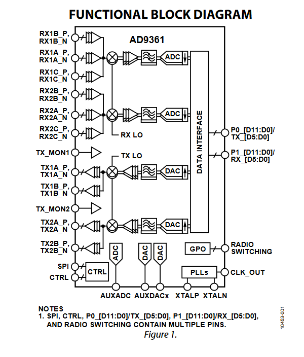
The AD9361 also has flexible manual gain modes that can be externally controlled. Two high dynamic range analog-to-digital converters (ADCs) per channel digitize the received I and Q signals and pass them through configurable decimation filters and 128-tap finite

impulse response (FIR) filters to produce a 12-bit output signal at the appropriate sample rate. The transmitters use a direct conversion architecture that achieves high modulation accuracy with ultralow noise. This transmitter design produces a best in class TX error vector magnitude (EVM) of <−40 dB, allowing significant system margin for the external power amplifier (PA) selection.

The on-board transmit (TX) power monitor can be used as a power detector, enabling highly accurate TX power measurements. The fully integrated phase-locked loops (PLLs) provide low power fractional-N frequency synthesis for all receive and transmit channels.

Channel isolation, demanded by frequency division duplex (FDD) systems, is integrated into the design. All VCO and loop filter components are integrated. The core of the AD9361 can be powered directly from a 1.3 V regulator.

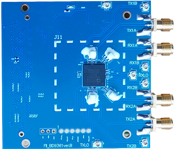
The IC is controlled via a standard 4-wire serial port and four real-time input/output control pins. Comprehensive power-down modes are included to minimize power consumption during normal use. The AD9361 is packaged in a 10 mm × 10 mm, 144-ball chip scale package ball grid array (CSP_BGA).

AD9361 Development Board

AD-FMCOMMS2-EBZ

The AD-FMCOMMS2-EBZ is a high-speed analog module designed to showcase the AD9361, a high performance, highly integrated RF transceiver intended for use in RF applications, such as 3G and 4G base station and test equipment applications, and software defined radios. Its programmability and wideband capability make it ideal for a broad range of transceiver applications. The device combines an RF front end with a flexible mixed-signal baseband section and integrated frequency synthesizers, simplifying design-in by providing a configurable digital interface to a processor or FPGA. The AD9361 chip operates in the 70 MHz to 6 GHz range, covering most licensed and unlicensed bands. The AD-FMCOMMS2-EBZ board comes specifically tuned and optimized to 2.4 GHz and due to the limitations of the on-board discrete external components, it may exhibit diminished RF performance on some other programmed configurations. The chip supports channel bandwidths from less than 200 kHz to 56 MHz by changing sample rate, digital filters, and decimation, all programmable within the AD9361 itself.

The AD-FMCOMMS2-EBZ provides RF engineers the ability to connect the AD9361 to a RF testbench (Vector Signal Analyzer, Signal generator, etc) and measure performance. The external components (which can easily be swapped) on the AD-FMCOMMS2-EBZ have a narrower RF tuning range 2400 – 2500 MHz. It is expected that most engineers will change these external components (pin for pin replacements from various vendors are available) for their specific application/frequency of interest. Anyone interested in a wider tuning range board should look at the AD-FMCOMMS3-EBZ.

AD Programming Kits Features

  • Software tunable across wide frequency range (70 MHz to 6.0 GHz) with a channel bandwidth of <200 kHz to 56 MHz.
  • Phase and frequency synchronization on both transmit and receive paths
  • Performance optimized for the narrowband range of 2.4GHz to 2.5GHz

AD9361 RF Transceiver

The FII-BD9361 board covers all features and benefits of AD9361. The AD9361 is a high performance, highly integrated radio frequency (RF) Agile Transceiver™ designed for use in 3G and 4G base station applications. Its programmability and wideband capability make it ideal for a broad range of transceiver applications.

Features and Benefits

  1. Software tunable across wide frequency range : TX :47 MHz to 6 GHz RX:70 MHz to 6 GHz
  2. Software tunable bandwidth: 200 kHz to 56 MHz.
  3. Software tunable TX Power and RX Dynamic Range:TX>80dB RX>70dB
  4. Powered up from single standard FMC connector
  5. Supports MIMO radio,2 ways TX and 2 ways RX(Max 4T4R by RF Switches configuration)
  6. Supports FII-7030 and other standard FMC Connector Platform software radio application

Product Details

  1. The FII-BD9361 is a high-speed analog module designed to showcase the AD9361, a high performance, highly integrated RF transceiver intended for use in RF applications, such as 3G and 4G base station and test equipment applications, and software defined radios. Its programmability and wideband capability make it ideal for a broad range of transceiver applications.
  2. The device combines an RF front end with a flexible mixed-signal baseband section and integrated frequency synthesizers, simplifying design-in by providing a configurable digital interface to a processor or FPGA. The AD9361 chip operates in the 70 MHz to 6 GHz range, covering most licensed and unlicensed bands. The chip supports channel bandwidths from less than 200 kHz to 56 MHz by changing sample rate, digital filters, and decimation, which are all programmable.

Interface:

Digital Interface:FMC-LPC
RF Interface: Four Way Differential Tranceiver

Features

TX band: 47 MHz to 6.0 GHz
RX band: 70 MHz to 6.0 GHz
Bandwidth Adjustment Range: 200 kHz to 56 MHz
Low noise figure: 2dB NF(noise figure/800MHz )
LO ,RX Gain Control,AGC
2.4Hhz local oscillator (LO) step
For more information, please check ad9361 introducation.

Applications

General purpose design  for any software-designed radio application
MIMO radio
Point to point communication systems
Femtocell/picocell/microcell base stations
USRP
3G/4G signal and protocol analysis
WiFi
ISM

3. Compatible Boards

FII-PE7030