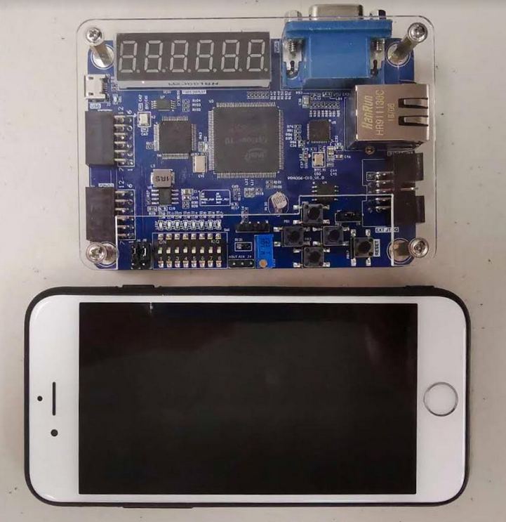
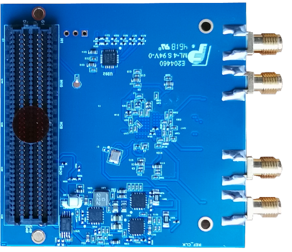
What is FPGA Development Board ?
Programmable logic technologies, such as field-programmable gate arrays (FPGAs), are an essential component of any modern circuit designer’s toolkit. With their expansive capabilities uniquely suited to a wide array of applications, FPGAs are ideal for solving many of the problems facing the rapidly evolving technology sector. The key benefits of programmable logic technologies include immense flexibility, cost savings over custom silicon, and increased performance by hardware parallelism.
For over a decade, we have proudly worked with Xilinx to expand our expertise and facilitate the development of new and exciting technology. We provide training and research platforms through our partnership with the Xilinx University Platform, enabling aspiring engineers the world over. Together, we look forward to empowering the next generation of circuit designers!
FPGA stands for field-programmable gate array. At its core, an FPGA is an array of interconnected digital subcircuits that implement common functions while also offering very high levels of flexibility. But getting a full picture of what an FPGA is requires more nuance. This article introduces the concepts behind FPGAs and briefly discuss what logic gates are, how to program an FPGA, and what makes an FPGA different from a microprocessor in design.
FPGA vs Microcontroller (Or, Why Use an FPGA When a Microcontroller Would Do?)
I think we can all agree that microcontrollers have become a dominant component in modern electronic design. They’re inexpensive and highly versatile, and nowadays they often serve as a person’s first introduction to the world of electronics. It’s natural for us to continue using components that we’re familiar with—and, as microcontrollers become increasingly powerful, there is less and less need to consider alternative solutions to our design challenges. Nonetheless, a microcontroller is built around a processor and processors come with fundamental limitations that need to be recognized and, in some cases, overcome.
So when would an engineer reach for an FPGA over a microcontroller? The answer comes down to software vs hardware.
A processor accomplishes its tasks by executing instructions in a sequential fashion. This means that the processor’s operations are inherently constrained: the desired functionality must be adapted to the available instructions and, in most cases, it is not possible to accomplish multiple processing tasks simultaneously.

When I first learned about FPGAs, all I really knew about before was microcontrollers. So first it is important to understand that they are very different devices. With a microcontroller, like an Arduino, the chip is already designed for you. You simply write some software, usually in C or C++, and compile it to a hex file that you load onto the microcontroller. The microcontroller stores the program in flash memory and will store it until it is erased or replaced. With microcontrollers you have control over the software.
FPGAs are different. You are the one designing the circuit. There is no processor to run software on, at least until you design one! You can configure an FPGA to be something as simple as an and gate, or something as complex as a multi-core processor. To create your design, you write some HDL (Hardware Description Language). The two most popular HDLs are Verilog and VHDL. You then synthesize your HDL into a bit file which you can use to configure the FPGA. A slight downside to FPGAs is that they store their configuration in RAM, not flash, meaning that once they lose power they lose their configuration. They must be configured every time power is applied.
That is not as bad as it seems as there are flash chips you can use that will automatically configure the stored bit file on power up. There are also some development boards which don’t require a programmer at all and will configure the FPGA at startup.
With FPGAs you have control over the hardware.
The Possibilities
With a typical microprocessor, you have dedicated pins for specific features. For example there will be only two pins on some microprocessors that are used as a serial port. If you want more than one serial port, or you want to use some other pins, your only solution besides getting a different chip is to use software to emulate a serial port. That works fine except you are wasting valuable processor time with the very basic task of sending out bits. If you want to emulate more than one port then you end up using all your processor time.
With an FPGA you are able to create the actual circuit, so it is up to you to decide what pins the serial port connects to. That also means you can create as many serial ports as you want. The only limitations you really have are the number of physical I/O pins and the size of the FPGA.
Just like microcontrollers that have a set amount of memory for your program, FPGAs can only emulate a circuit so large.
One of the very interesting things about FPGAs is that while you are designing the hardware, you can design the hardware to be a processor that you then can write software for! In fact, companies that design digital circuits, like Intel or nVidia, often use FPGAs to prototype their chips before creating them.
FPGA Applications
Due to their programmable nature, FPGAs are an ideal fit for many different markets. As the industry leader, Xilinx provides comprehensive solutions consisting of FPGA devices, advanced software, and configurable, ready-to-use IP cores for markets and applications such as:
- Aerospace & Defense – Radiation-tolerant FPGAs along with intellectual property for image processing, waveform generation, and partial reconfiguration for SDRs.
- ASIC Prototyping – ASIC prototyping with FPGAs enables fast and accurate SoC system modeling and verification of embedded software
- Audio – Xilinx FPGAs and targeted design platforms enable higher degrees of flexibility, faster time-to-market, and lower overall non-recurring engineering costs (NRE) for a wide range of audio, communications, and multimedia applications.
- Automotive – Automotive silicon and IP solutions for gateway and driver assistance systems, comfort, convenience, and in-vehicle infotainment. – Learn how Xilinx FPGA’s enable Automotive Systems
- Broadcast & Pro AV – Adapt to changing requirements faster and lengthen product life cycles with Broadcast Targeted Design Platforms and solutions for high-end professional broadcast systems.
- Consumer Electronics – Cost-effective solutions enabling next generation, full-featured consumer applications, such as converged handsets, digital flat panel displays, information appliances, home networking, and residential set top boxes.
- Data Center – Designed for high-bandwidth, low-latency servers, networking, and storage applications to bring higher value into cloud deployments.
- High Performance Computing and Data Storage – Solutions for Network Attached Storage (NAS), Storage Area Network (SAN), servers, and storage appliances.
- Industrial – Xilinx FPGAs and targeted design platforms for Industrial, Scientific and Medical (ISM) enable higher degrees of flexibility, faster time-to-market, and lower overall non-recurring engineering costs (NRE) for a wide range of applications such as industrial imaging and surveillance, industrial automation, and medical imaging equipment.
- Medical – For diagnostic, monitoring, and therapy applications, the Virtex FPGA and Spartan® FPGA families can be used to meet a range of processing, display, and I/O interface requirements.
- Security – Xilinx offers solutions that meet the evolving needs of security applications, from access control to surveillance and safety systems.
- Video & Image Processing – Xilinx FPGAs and targeted design platforms enable higher degrees of flexibility, faster time-to-market, and lower overall non-recurring engineering costs (NRE) for a wide range of video and imaging applications.
- Wired Communications – End-to-end solutions for the Reprogrammable Networking Linecard Packet Processing, Framer/MAC, serial backplanes, and more
- Wireless Communications – RF, base band, connectivity, transport and networking solutions for wireless equipment, addressing standards such as WCDMA, HSDPA, WiMAX and others.
