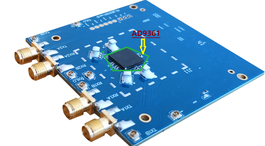
FII-AD9371 (completely compatible with ADRV9371-W/PCBZ ) are radio cards designed to showcase the AD9371, a high performance wideband integrated RF transceiver intended for use in RF applications such as 4G basestation, test and measurement applications and software defined radios. Transceiver For Use With AD9371, AD9528, ADP5054
The radio cards provide hardware engineers, software engineers and system architects with a single 2×2 transceiver platform for device evaluation and rapid prototyping of radio solutions.
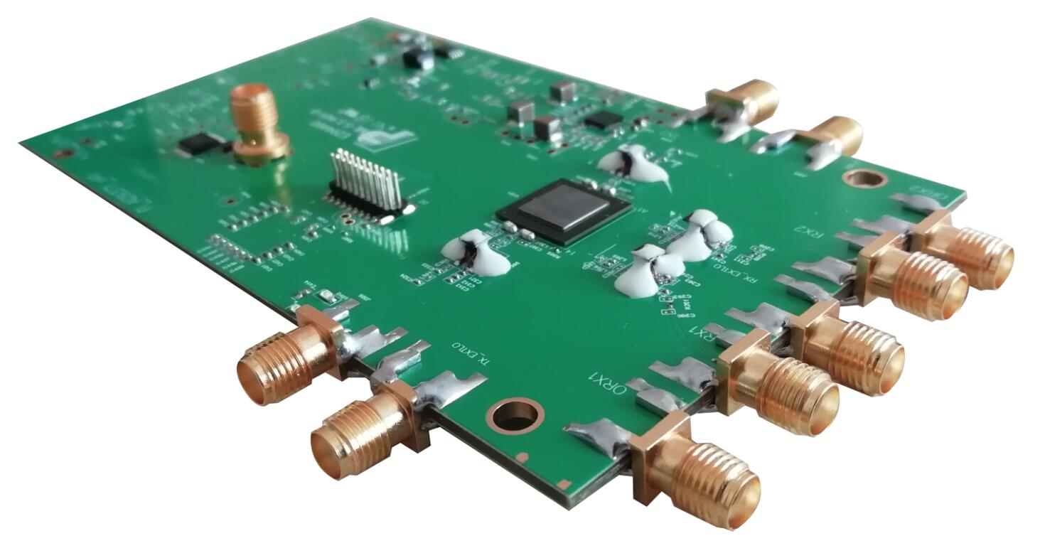
All peripherals necessary for the radio card to operate including a high efficiency switcher only power supply solution, and a high performance clocking solution are populated on the board.
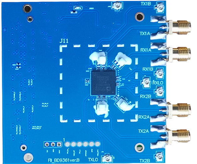
- Complete Radio Card platform containing AD9371 with:
- 2 x Transmit outputs
- 2 x Receive inputs
- 2 x Observation inputs
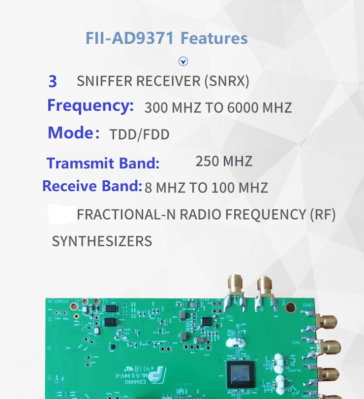
- 1x Sniffer path
- Narrow tuning range and Wide tuning range options
- ADRV9371-W/PCBZ matched for 300MHz – 6GHz
- Complete with high efficiency power supply solution and clocking solution for AD9371
- FMC connector to Xilinx ZC706 motherboard (EK-Z7-ZC706-G).
- Powered from single FMC connector
- Includes schematics, layout, BOM, HDL, drivers and application software
| Frequency | 300MHz ~ 6GHz |
|---|
| Type | Transceiver |
|---|
| Base Part Number | ADRV9371 |
|---|
| For Use With/Related Products | AD9371, AD9528, ADP5054 |
|---|
| Datasheets | |
|---|---|
| Video File | GNU Radio Conference 2016 – Radio Architecture Design Challenges |
If you have any questions, you can contact us or post in the FII-AD9361 product forums. If you can not register to post, please let us know and I will create a forum username for you.
ADRV9371-N/PCBZ Product Details
The ADRV9371-N/PCBZ and ADRV9371-WPCBZ are radio cards designed to showcase the AD9371, a high performance wideband integrated RF transceiver intended for use in RF applications such as 4G basestation, test and measurement applications and software defined radios.
The radio cards provide hardware engineers, software engineers and system architects with a single 2×2 transceiver platform for device evaluation and rapid prototyping of radio solutions.
All peripherals necessary for the radio card to operate including a high efficiency switcher only power supply solution, and a high performance clocking solution are populated on the board.
Both narrow tuning range and wide tuning range options exist.
The ADRV9371-N/PCBZ is optimized for performance over a narrow tuning range1.8GHz – 2.6GHz. It will exhibit diminished RF performance on tuned RF frequencies outside of this band. This board is primarily intended to provide RF engineers with the ability to connect the AD9371 to an RF test bench (Vector Signal Analyzer, Signal Generator, etc) and achieve its optimum performance.
People who follow the flow that is outlined, have a much better experience with things. However, like many things, documentation is never as complete as it should be. If you have any questions, feel free to ask.
-
Use the board to better understand the AD9371/AD9375
-
What you need to get started
-
Quick Start Guides
-
Linux on ZC706
-
Configure a pre-existing SD-Card
-
Update the old card you received with your hardware
-
-
Linux Applications
-
IIO Scope
-
AD9371/AD9375 IIO Scope View
-
AD9371/AD9375 Control IIO Scope Plugin
-
Advanced AD9371/AD9375 Control IIO Scope Plugin
-
-
FRU EEPROM Utility
-
-
Push custom data into/out of the AD9371/AD9375
-
Basic Data files and formats
-
Stream data into/out of MATLAB
-
Python Interfaces
-
-
-
Design with the AD9371/AD9375
-
Understanding the AD9371/AD9375
-
AD9371 Product page
-
AD9375 Product page
-
Full Datasheet and chip design package
-
MATLAB Filter Wizard / Profile Generator for AD9371
-
-
Hardware in the Loop / How to design your own custom BaseBand
-
GNU Radio
-
Transceiver Toolbox
-
-
Design a custom AD9371/AD9375 based platform
-
Linux software
-
AD9371/AD9375 Linux Device Driver
-
Customizing the devicetree on the target
-
-
AD9528 Low Jitter Clock Generator Linux Driver
-
AD7291 IIO ADC Linux Driver
-
JESD204B Transmit Linux Driver
-
JESD204B Status Utility
-
-
JESD204B Receive Linux Driver
-
JESD204B Status Utility
-
-
AXI JESD204B GT HDL Linux Driver
-
JESD204 Eye Scan
-
-
AXI ADC HDL Linux Driver
-
AXI DAC HDL Linux Driver
-
-
Changing the VCXO frequency and updating the default RF Transceiver Profile
-
AD9371/AD9375 No-OS System Level Design Setup
-
HDL Reference Design which you must use in your FPGA.
-
Transceiver Toolbox: HDL Targeting with MATLAB and Simulink
-
-
-
Additional Documentation about SDR Signal Chains – The math behind the RF
-
Help and Support
AD9371 Prototyping Platforms
ADRV9371-N/PCBZ and ADRV9371-W/PCBZ Prototyping Platforms using the AD9371 Integrated, Dual RF Transceiver with Observation Path
Analog Devices Inc.
The ADRV9371-W/PRBZ, ADRV9371-N/PCBZ are FMC radio cards for the AD9371, a highly integrated RF Transceiver™. While the complete chip level design package can be found on the ADI web site, information on the card and how to use it, the design package that surrounds it, and the software which can make it work can be found here.
Prerequisites for AD9371 based boards
What you need, depends on what you are trying to do. As a minimum, you need to start out with:
-
The AD9371 based card.
-
A carrier platform. ADI does not offer these boards for sale or loan, getting one yourself is normal part of development or evaluation of the AD9371. Our recommended carriers (the ones we use all the time) are either:
-
The Xilinx ZC706. The fabric on this device is much larger, and if you are looking at targeting – this is the recommended option.
-
There are a few more boards, which do work, but are currently not yet supported. The experience of the fabric only solutions is very close to the ARM/FPGA SoC based solutions, but the GUI runs on a host PC (Windows or Linux).
-
Supported Carriers
The ADRV9371/PCBZ is, by definition a “FPGA mezzanine card” (FMC), that means it needs a carrier to plug into. The carriers we support are:
Board ADRV9371-N/PCBZ ADRV9371-W/PCBZ ADRV9375-N/PCBZ ZCU102 √ √ √ KCU105 √ √ √ ZC706 √ √ √ Arria 10 SoC √ √ √ Arria 10 GX √ √ √
-
-
some way to interact with the platform,
-
for the ARM/FPGA SoC platforms, this normally includes:
-
HDMI monitor (1080p is best) or VGA Monitor
-
USB Keyboard
-
USB Mouse
-
-
for the FPGA only solutions, this includes:
-
LAN cable (Ethernet)
-
Host PC (Windows or Linux)
-
-
-
Internet connection (without proxies makes things much easier) to update the scripts/binaries on the SD Card that came with the ADI FMC Card. (Firewalls are OK, proxies make things a pain).
-
RF Test equipment