A field-programmable gate array (FPGA) is an integrated circuit designed to be configured by a customer or a designer after manufacturing – hence the term “field-programmable”.
The FPGA configuration is generally specified using a hardware description language (HDL), similar to that used for an Application-Specific Integrated Circuit (ASIC). Circuit diagrams were previously used to specify the configuration, but this is increasingly rare due to the advent of electronic design automation tools.
FII was founded on making FPGA technology more approachable for students or FPGA beginners to learn. We partnered with the world leader and founder of modern day FPGA technology, Altera and Xilinx, to create platforms that were ideally suited for learning.
Below are boards that we recommend for beginning users. These boards have course material, books, and tutorials to get you started!
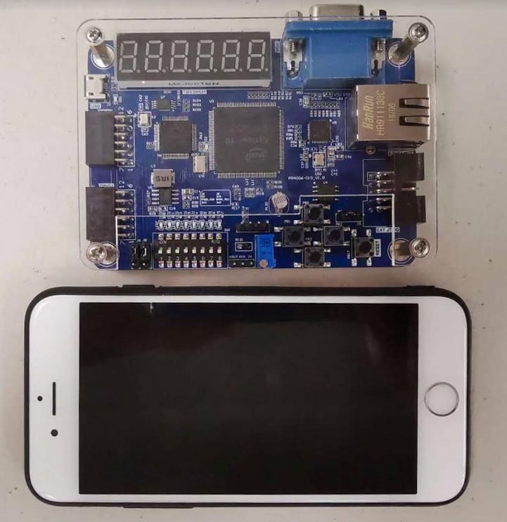
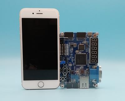
Altera FPGA Study Board, Verilog for beginner – Cyclone-10 FPGA Development Board – $59
The advantage of FPGA beginner study board:
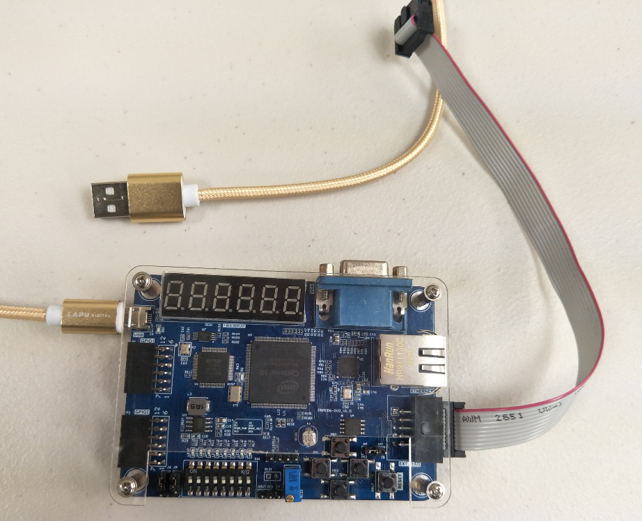
- Beginner FPGA study board, cheaper but fully functional. cellphone sized. ( < 80 USD )
- power supply and download at the same time, no extra power supply and no extra data transfer line needed
- Small volume and light and can be put into your pocket. size: 10cm X 7 cm.
- Unique function: can be a study board as well a multifunctional JTAG downloader.
- We use newest version Intel FPGA within two years and you can always keep in the front of FPGA industry.
FII-PRA006 is both a FPGA development board and a JTAG down-loader. As a JTAG down-loader, It support:
- Intel(Altera) FPGA:Support Quartus II5.0 and all the version afterwords;
- Xilinx FPGA:Support ISE9.0 and all version afterwords or All Vivado versions;
- Compatible with ARM Cortext:Support OpenOCD
- RISC-V CPU:Support FreeDomStudio,including GCC、OpenOCD、and GDB Debugging
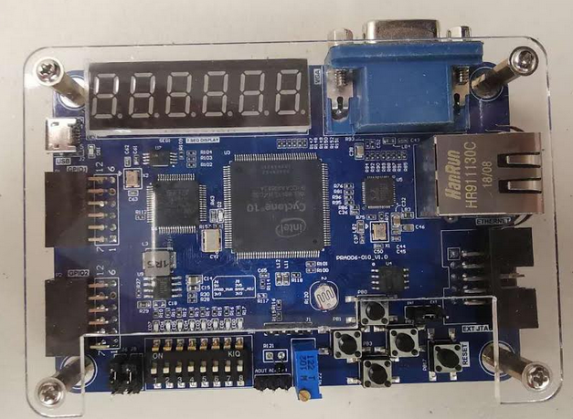
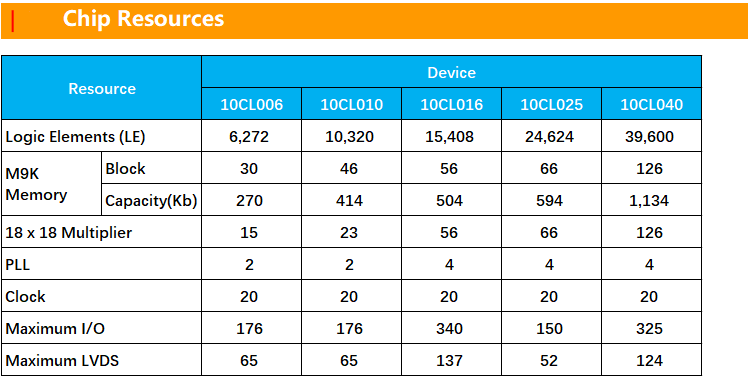
Altera FPGA Study Board Hardware Resources:
- 6 seven_seg_r
- VGA Video Interface × 1
- 1G Ethernet Interface × 1
- I2C EEPROM × 1
- DIP Switch × 8
- Controllable LED light × 8
- Photoresistance × 1
- Thermistor × 1
- Adjustable Varistor × 1
- Buttons × 4
- GPIO Interface × 2
- Micro usb Interface(Power Supply and downlaod ) × 1
- SPI Communication Interface × 1
- AD/DA Conversion chip × 1
- JTAG Download Interface × 1
- FLASH 32Mbit × 1
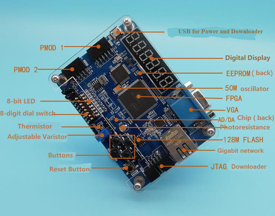
The Biggest Hardware Benefits:
-
- USB port for power supply, downloader, communications ;
- One 50M Oscillator. A stable clock for development board;
- 6-digit common anode digital tube,display the data by dynamic scan;
- 1 VGA port to display picture and video;
- 1 I2C port EEPROM chip,Model: AT24C02;
- 1 adaptive 10M, 100M/1000M Ethernet port;
- 5 buttons,4 for programmable buttons , and one button for resetting;
- 1 Photoresistance. It can be used for simulating light control;
- 1 thermistor. It can be used for collecting temperature or simulating alarm function
- An adjustable resistor can simulate voltage changes, etc.
- 1 PCF8591 AD/DA Conversion chip;
- 8-digit dial switch;
- 8-bit LED light-emitting diode;
- One 128Mbit Flash Chip;
- 2 GPIO external port for communication extension port ;
- One JTAGPort , and make PRA006/010 a functional JTAG down-loader, can be used as a JTAG downloader for Intel,Xilinx and other FPGA downloadable program;
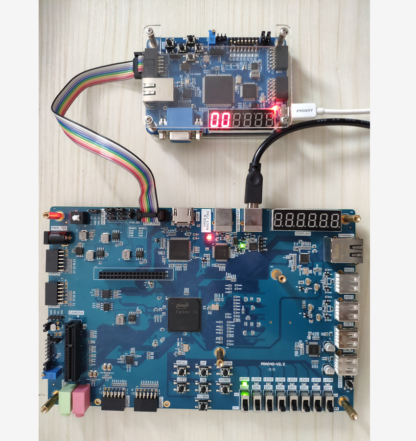
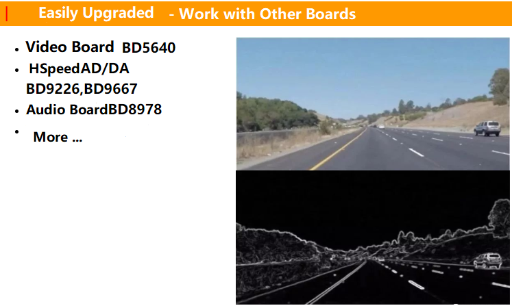
It can also be used with other FPGA development Boards:


Official Shopping Websites
https://fpgamarketing.com/Altera-FPGA-Study-Board-Verilog-for-beginner-Cyclone-10-FPGA-FII-PRA006.htm
FPGA for Beginner Tutorial – FPGA Experimental Manuals
- FPGA Board for beginner – FII-PRA006/010 Hardware Reference Guide
- FPGA Beginner Tutorial – Ethernet Experiment – FPGA Board for Beginner – Experiment 14
- FPGA Beginner Tutorial – VGA Experiment – FPGA Board for Beginner – Experiment 13
- FPGA Beginner Tutorial – AD, DA Experiment – FPGA Board for Beginner – Experiment 12
- FPGA Beginner Tutorial – IIC Protocol Transmission – FPGA Board for Beginner – Experiment 11
- FPGA Tutorial – Asynchronous Serial Port Design and Experiment – FPGA for Beginner – Experiment 10
- FPGA Tutorial – Use Dual-port RAM to Read and Write Frame Data – FPGA Board for Beginner – Experiment 9
- FPGA Tutorial – Use of ROM (Read-only Memory) – FPGA Board for Beginner – Experiment 8
- FPGA Tutorial – Hexadecimal Numbers to BCD Code Conversion and Application – FPGA Board for Beginner – Experiment 7
- FPGA Tutorial – Use Multiplier and ModelSim – FPGA Board for Beginner – Experiment 6
- FPGA tutorial – Block_debouncing – FBGA Board for for beginner – Experiment 5
- FPGA Tutorial – Block/ Schematic Test – FPGA Board for Beginner – Experiment 4
- FPGA for Beginner Tutorial – Experiment 3 – BCD_counter – FII-PRA006
- FPGA for Beginner Tutorial – Experiment 2 Switch and Use SignalTap II – FII-PRA006
- FPGA Board Beginner Tutorial – FII-PRA006 Experiment 1 LED_shifting
FPGAs provide benefits to designers of many types of electronic equipment, ranging from IOT, smart homes, smart energy grids, aircraft navigation, automotive driver’s assistance, medical ultrasounds and data center search engines, and so on.
We will send you experimental manuals when you have bought our pocket study board. PRA006 or PRA010
What is FPGA?
FPGA stands for “Field Programmable Gate Array“. As you may already know, FPGA essentially is a huge array of gates which can be programmed and reconfigured any time anywhere. “Huge array of gates” is an oversimplified description of FPGA. FPGA is indeed much more complex than a simple array of gates.
Some FPGAs has built-in hard blocks such as Memory controllers, high-speed communication interfaces, PCIe Endpoints, etc. But the point is, there are a lot of gates inside the FPGA which can be arbitrarily connected together to make a circuit of your choice. More or less like connecting individual logic gate ICs (again oversimplified but a good mental picture nonetheless).
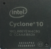
FPGAs are manufactured by companies like Xilinx, Altera, Microsemi, etc… FPGAs are fundamentally similar to CPLDs but CPLDs are very small in size and capability compared to FPGAs.
What are the applications of FPGA?
Architecturally FPGAs are essentially a sea of gates which can be reconfigured to build almost any digital circuit that one can imagine.
This great flexibility along with the ability to reconfigure the device with different designs at-will makes FPGA a better choice compared to ASICs (Application Specific Integrated Circuit) for a lot of applications. For example, deep learning, AI or application acceleration system can re-program a single FPGA with different algorithms at different times to achieve the best performance. An ASIC would not be as flexible in such situations.
In certain applications, the number of individual units manufactured would be very small. Designing and manufacturing ASICs for these applications can be prohibitively expensive. In such situations, FPGA can offer very cost effective but robust solutions. The module form-factor boards such as the Narvi Spartan 7 FPGA Module make it easier to implement the applications without requiring end-product designers to take care of complex details such as FPGA power supplies, DDR3 routing, etc. Below are some of the potential applications of FPGAs in no particular order.
-
- Cryptography
- ASIC prototyping
- Industrial, medical and Scientific Instruments
- Audio/Video and Image processing and broadcasting
- High-performance computing, AI, and Deep Learning
- Military and Space applications
- Networking, packet processing, and other communications
What is FPGA programming?
FPGA programming or FPGA development process is the process of planning, designing and implementing a solution on FPGA. The amount and type of planning vary from application to application. But creating a requirements document that captures all specific requirements and creating a design document that explains how the proposed solution would be implemented can be very helpful to enumerate potential problems and plan around them. A little bit of time spent creating a quality design document will save tons of time in refactoring, debugging and bug fixing later. Implementing a solution on FPGA includes building the design using one of the design entry methods such as schematics or HDL code such as Verilog or VHDL, Synthesizing the design (Synthesis, netlist generation, place and route etc..) in to output files that FPGAs can understand and program the output file to the physical FPGA device using programming tools. Entering the design using schematics is not used in the industry widely anymore. So we will keep the discussion limited to design entry using HDL (Hardware Description Language), specifically Verilog in this article series. Synthesis and programming are almost completely taken care of the vendor tools such as ISE and Vivado and Numato Lab configuration tools. All necessary steps to be taken by the user as part of design entry, synthesis and programming will be explained in subsequent sections.
The Benefits of FPGA
Flexibility
- FPGA functionality can change upon every power-up of the device. So, when a design engineer wants to make a change, they can simply download a new configuration file into the device and try out the change.
- Often, changes can be made to the FPGA without making costly PC board changes.
- ASSPs and ASICs have fixed hardware functionality that can’t be changed without great cost and time.
Acceleration
- FPGAs are sold “off the shelf” vs. ASICs (which require manufacturing cycles taking many months).
- Because of FPGA flexibility, OEMs can ship systems as soon as the design is working and tested.
- FPGAs provide off-load and acceleration functions to CPUs, effectively speeding up the entire system performance.
Integration
Today’s FPGAs include on-die processors, transceiver I/O’s at 28 Gbps (or faster), RAM blocks, DSP engines, and more. More functions within the FPGA mean fewer devices on the circuit board, increasing reliability by reducing the number of device failures.
Total Cost of Ownership (TCO)
- While ASICs may cost less per unit than an equivalent FPGA, building them requires a non-recurring expense (NRE), expensive software tools, specialized design teams, and long manufacturing cycles.
- Intel FPGAs support long lifecycles (15-years or more), avoiding the cost of redesigning and requalifying OEM production equipment if one of the electronic devices on-board goes end of life (EOL).
- FPGAs reduce risk, allowing prototype systems to ship to customers for field trials, while still providing the ability to make changes quickly before ramping to volume production.
The concept behind an FPGA’s programmability is a basic building block containing various logic types that are connected and interconnected to perform any logic function. “Basic building block” is a generic term that I’m using, but you may hear terms like “logic cells,” “combinational logic blocks” (CLBs), or “logic array blocks” (LABs); it depends on the manufacturer. The basic building block contains logic resources and is the starting point that the FPGA uses to constructs the design.
The experimental manual of FII-PRA006 pocket Board for beginners
The Hardware Configuration of FII-PRA006 Board for beginners
The Schematic Diagram of FII-PRA006 FPGA Board for beginners
We will send you above documents after you have bought our PRA006 pocket study board.
Extension Experiments
Video Camera
- Pictures and Videos Collection
- Edge check and human-face location Positioning
- Picture and video Zip and UnZip
Voice and Speech
- voice and speech collection
- Speech Recognition
- High Speed Analog signal acquisition
Risc-V
- Low level CPU programing
- Run C language
- C language debugging onboard device